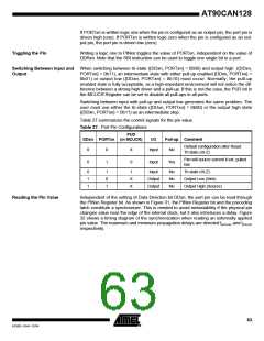
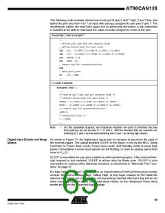
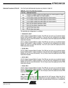
AT90CAN128
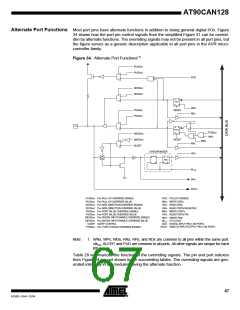
Alternate Port Functions Most port pins have alternate functions in addition to being general digital I/Os. Figure
34 shows how the port pin control signals from the simplified Figure 31 can be overrid-
den by alternate functions. The overriding signals may not be present in all port pins, but
the figure serves as a generic description applicable to all port pins in the AVR micro-
controller family.
Figure 34. Alternate Port Functions(1)
PUOExn
PUOVxn
1
PUD
0
DDOExn
DDOVxn
1
Q
D
0
DDxn
Q CLR
WDx
RDx
PVOExn
PVOVxn
RESET
1
0
1
0
Pxn
Q
D
PORTxn
PTOExn
WPx
Q CLR
DIEOExn
DIEOVxn
SLEEP
RESET
WRx
1
0
RRx
RPx
SYNCHRONIZER
SET
D
Q
D
L
Q
Q
PINxn
CLR Q
CLR
clk I/O
DIxn
AIOxn
PUOExn: Pxn PULL-UP OVERRIDE ENABLE
PUOVxn: Pxn PULL-UP OVERRIDE VALUE
PUD: PULLUP DISABLE
WDx: WRITE DDRx
RDx: READ DDRx
DDOExn: Pxn DATA DIRECTION OVERRIDE ENABLE
DDOVxn: Pxn DATA DIRECTION OVERRIDE VALUE
PVOExn: Pxn PORT VALUE OVERRIDE ENABLE
PVOVxn: Pxn PORT VALUE OVERRIDE VALUE
RRx: READ PORTx REGISTER
WRx: WRITE PORTx
RPx: READ PORTx PIN
WPx: WRITE PINx
DIEOExn: Pxn DIGITAL INPUT-ENABLE OVERRIDE ENABLE
DIEOVxn: Pxn DIGITAL INPUT-ENABLE OVERRIDE VALUE
SLEEP: SLEEP CONTROL
clkI/O
DIxn: DIGITAL INPUT PIN n ON PORTx
AIOxn: ANALOG INPUT/OUTPUT PIN n ON PORTx
: I/O CLOCK
PTOExn: Pxn, PORT TOGGLE OVERRIDE ENABLE
Note:
1. WRx, WPx, WDx, RRx, RPx, and RDx are common to all pins within the same port.
clkI/O, SLEEP, and PUD are common to all ports. All other signals are unique for each
pin.
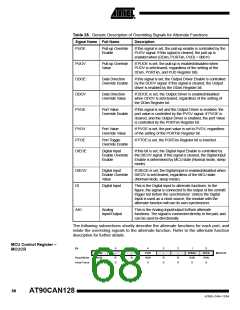
Table 28 summarizes the function of the overriding signals. The pin and port indexes
from Figure 34 are not shown in the succeeding tables. The overriding signals are gen-
erated internally in the modules having the alternate function.
67
4250E–CAN–12/04

 ATMEL [ ATMEL ]