AT90CAN128
SRAM Data Memory
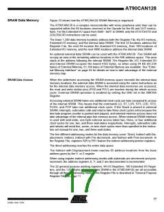
Figure 10 shows how the AT90CAN128 SRAM Memory is organized.
The AT90CAN128 is a complex microcontroller with more peripheral units than can be
supported within the 64 locations reserved in the Opcode for the IN and OUT instruc-
tions. For the Extended I/O space from 0x60 - 0xFF in SRAM, only the ST/STS/STD and
LD/LDS/LDD instructions can be used.
The lower 1,280 data memory locations address both the Register File, the I/O memory,
Extended I/O memory, and the internal data SRAM. The first 32 locations address the
Register File, the next 64 location the standard I/O memory, then 160 locations of
Extended I/O memory, and the next 4096 locations address the internal data SRAM.
An optional external data SRAM can be used with the AT90CAN128. This SRAM will
occupy an area in the remaining address locations in the 64K address space. This area
starts at the address following the internal SRAM. The Register file, I/O, Extended I/O
and Internal SRAM occupies the lowest 4352 bytes, so when using 64 KB (65,536
bytes) of External Memory, 61,184 bytes of External Memory are available. See “Exter-
nal Memory Interface” on page 24 for details on how to take advantage of the external
memory map.
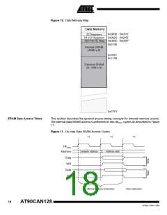
SRAM Data Access
When the addresses accessing the SRAM memory space exceeds the internal data
memory locations, the external data SRAM is accessed using the same instructions as
for the internal data memory access. When the internal data memories are accessed,
the read and write strobe pins (PG0 and PG1) are inactive during the whole access
cycle. External SRAM operation is enabled by setting the SRE bit in the XMCRA
Register.
Accessing external SRAM takes one additional clock cycle per byte compared to access
of the internal SRAM. This means that the commands LD, ST, LDS, STS, LDD, STD,
PUSH, and POP take one additional clock cycle. If the Stack is placed in external
SRAM, interrupts, subroutine calls and returns take three clock cycles extra because the
two-byte program counter is pushed and popped, and external memory access does not
take advantage of the internal pipe-line memory access. When external SRAM interface
is used with wait-state, one-byte external access takes two, three, or four additional
clock cycles for one, two, and three wait-states respectively. Interrupts, subroutine calls
and returns will need five, seven, or nine clock cycles more than specified in the instruc-
tion set manual for one, two, and three wait-states.
The five different addressing modes for the data memory cover: Direct, Indirect with Dis-
placement, Indirect, Indirect with Pre-decrement, and Indirect with Post-increment. In
the Register File, registers R26 to R31 feature the indirect addressing pointer registers.
The direct addressing reaches the entire data space.
The Indirect with Displacement mode reaches 63 address locations from the base
address given by the Y- or Z-register.
When using register indirect addressing modes with automatic pre-decrement and post-
increment, the address registers X, Y, and Z are decremented or incremented.
The 32 general purpose working registers, 64 I/O Registers, 160 Extended I/O Regis-
ters, and the 1,024 bytes of internal data SRAM in the AT90CAN128 are all accessible
through all these addressing modes. The Register File is described in “General Purpose
Register File” on page 11.
17
4250E–CAN–12/04

 ATMEL [ ATMEL ]