AT90CAN128
The Timer/Counter Overflow Flag (TOV0) is set each time the counter reaches MAX. If
the interrupt is enabled, the interrupt handler routine can be used for updating the com-
pare value.
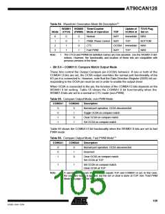
In fast PWM mode, the compare unit allows generation of PWM waveforms on the
OC0A pin. Setting the COM0A1:0 bits to two will produce a non-inverted PWM and an
inverted PWM output can be generated by setting the COM0A1:0 to three (See Table 56
on page 105). The actual OC0A value will only be visible on the port pin if the data direc-
tion for the port pin is set as output. The PWM waveform is generated by setting (or
clearing) the OC0A Register at the compare match between OCR0A and TCNT0, and
clearing (or setting) the OC0A Register at the timer clock cycle the counter is cleared
(changes from MAX to BOTTOM).
The PWM frequency for the output can be calculated by the following equation:
fclk_I/O
fOCnxPWM = -----------------
N ⋅ 256
The N variable represents the prescale factor (1, 8, 64, 256, or 1024).
The extreme values for the OCR0A Register represents special cases when generating
a PWM waveform output in the fast PWM mode. If the OCR0A is set equal to BOTTOM,
the output will be a narrow spike for each MAX+1 timer clock cycle. Setting the OCR0A
equal to MAX will result in a constantly high or low output (depending on the polarity of
the output set by the COM0A1:0 bits.)
A frequency (with 50% duty cycle) waveform output in fast PWM mode can be achieved
by setting OC0A to toggle its logical level on each compare match (COM0A1:0 = 1). The
waveform generated will have a maximum frequency of fOC0A = fclk_I/O/2 when OCR0A is
set to zero. This feature is similar to the OC0A toggle in CTC mode, except the double
buffer feature of the Output Compare unit is enabled in the fast PWM mode.
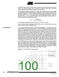
Phase Correct PWM Mode
The phase correct PWM mode (WGM01:0 = 1) provides a high resolution phase correct
PWM waveform generation option. The phase correct PWM mode is based on a dual-
slope operation. The counter counts repeatedly from BOTTOM to MAX and then from
MAX to BOTTOM. In non-inverting Compare Output mode, the Output Compare (OC0A)
is cleared on the compare match between TCNT0 and OCR0A while upcounting, and
set on the compare match while downcounting. In inverting Output Compare mode, the
operation is inverted. The dual-slope operation has lower maximum operation frequency
than single slope operation. However, due to the symmetric feature of the dual-slope
PWM modes, these modes are preferred for motor control applications.
The PWM resolution for the phase correct PWM mode is fixed to eight bits. In phase
correct PWM mode the counter is incremented until the counter value matches MAX.
When the counter reaches MAX, it changes the count direction. The TCNT0 value will
be equal to MAX for one timer clock cycle. The timing diagram for the phase correct
PWM mode is shown on Figure 43. The TCNT0 value is in the timing diagram shown as
a histogram for illustrating the dual-slope operation. The diagram includes non-inverted
and inverted PWM outputs. The small horizontal line marks on the TCNT0 slopes repre-
sent compare matches between OCR0A and TCNT0.
101
4250E–CAN–12/04

 ATMEL [ ATMEL ]