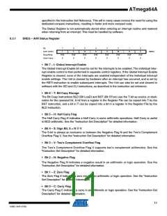
ATmega64A
2.3.9
Port G (PG4:PG0)
Port G is a 5-bit bi-directional I/O port with internal pull-up resistors (selected for each bit). The
Port G output buffers have symmetrical drive characteristics with both high sink and source
capability. As inputs, Port G pins that are externally pulled low will source current if the pull-up
resistors are activated. The Port G pins are tri-stated when a reset condition becomes active,
even if the clock is not running.
Port G also serves the functions of various special features.
In ATmega103 compatibility mode, these pins only serves as strobes signals to the external
memory as well as input to the 32 kHz Oscillator, and the pins are initialized to PG0 = 1,
PG1 = 1, and PG2 = 0 asynchronously when a reset condition becomes active, even if the clock
is not running. PG3 and PG4 are Oscillator pins.
2.3.10
RESET
Reset input. A low level on this pin for longer than the minimum pulse length will generate a
reset, even if the clock is not running. The minimum pulse length is given in Table 28-3 on page
330. Shorter pulses are not guaranteed to generate a reset.
2.3.11
2.3.12
2.3.13
XTAL1
XTAL2
AVCC
Input to the inverting Oscillator amplifier and input to the internal clock operating circuit.
Output from the inverting Oscillator amplifier.
AVCC is the supply voltage pin for Port F and the A/D Converter. It should be externally con-
nected to VCC, even if the ADC is not used. If the ADC is used, it should be connected to VCC
through a low-pass filter.
2.3.14
2.3.15
AREF
PEN
AREF is the analog reference pin for the A/D Converter.
This is a programming enable pin for the SPI Serial Programming mode. By holding this pin low
during a Power-on Reset, the device will enter the SPI Serial Programming mode. PEN is inter-
nally pulled high. The pullup is shown in Figure 10-1 on page 52 and its value is given in Section
28.2 “DC Characteristics” on page 327. PEN has no function during normal operation.
3. Resources
A comprehensive set of development tools, application notes and datasheetsare available for
download on http://www.atmel.com/avr.
Note:
1.
4. Data Retention
Reliability Qualification results show that the projected data retention failure rate is much less
than 1 PPM over 20 years at 85°C or 100 years at 25°C.
7
8160C–AVR–07/09

 ATMEL [ ATMEL ]