ATmega64A
12.1.3
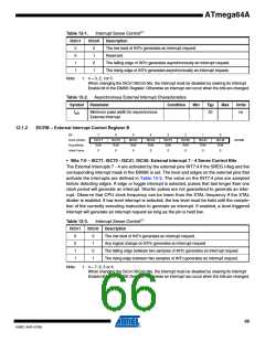
EIMSK – External Interrupt Mask Register
Bit
7
6
5
4
3
2
1
0
0x39 (0x59)
Read/Write
Initial Value
INT7
R/W
0
INT6
R/W
0
INT5
R/W
0
INT4
R/W
0
INT3
R/W
0
INT2
R/W
0
INT1
R/W
0
INT0
R/W
0
EIMSK
• Bits 7:4 – INT7 - INT0: External Interrupt Request 7 - 0 Enable
When an INT7 - INT4 bit is written to one and the I-bit in the Status Register (SREG) is set (one),
the corresponding external pin interrupt is enabled. The Interrupt Sense Control bits in the Exter-
nal Interrupt Control Registers – EICRA and EICRB defines whether the External Interrupt is
activated on rising or falling edge or level sensed. Activity on any of these pins will trigger an
interrupt request even if the pin is enabled as an output. This provides a way of generating a
software interrupt.
12.1.4
EIFR – External Interrupt Flag Register
Bit
0x38 (0x58)
7
6
5
INTF5
R/W
0
4
INTF4
R/W
0
3
INTF3
R/W
0
2
INTF2
R/W
0
1
INTF1
R/W
0
0
INTF0
R/W
0
INTF7
INTF6
R/W
0
EIFR
Read/Write
Initial Value
R/W
0
• Bits 7:0 – INTF7 - INTF0: External Interrupt Flags 7 - 0
When an edge or logic change on the INT7:0 pin triggers an interrupt request, INTF7:0 becomes
set (one). If the I-bit in SREG and the corresponding Interrupt Enable bit, INT7:0 in EIMSK, are
set (one), the MCU will jump to the Interrupt Vector. The flag is cleared when the interrupt rou-
tine is executed. Alternatively, the flag can be cleared by writing a logical one to it. These flags
are always cleared when INT7:0 are configured as level interrupt. Note that when entering sleep
mode with the INT3:0 interrupts disabled, the input buffers on these pins will be disabled. This
may cause a logic change in internal signals which will set the INTF3:0 flags. See “Digital Input
Enable and Sleep Modes” on page 72 for more information.
67
8160C–AVR–07/09

 ATMEL [ ATMEL ]