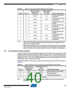
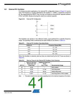
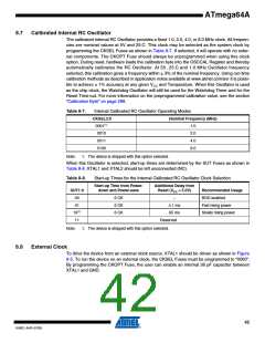
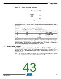
ATmega64A
8.10 Register Descriprion
8.10.1
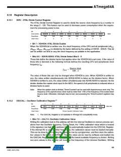
XDIV – XTAL Divide Control Register
The XTAL Divide Control Register is used to divide the source clock frequency by a number in
the range 2 - 129. This feature can be used to decrease power consumption when the require-
ment for processing power is low.
Bit
7
XDIVEN
R/W
0
6
XDIV6
R/W
0
5
XDIV5
R/W
0
4
XDIV4
R/W
0
3
XDIV3
R/W
0
2
XDIV2
R/W
0
1
XDIV1
R/W
0
0
XDIV0
R/W
0
0x3C (0x5C)
Read/Write
Initial Value
XDIV
• Bit 7 – XDIVEN: XTAL Divide Enable
When the XDIVEN bit is written one, the clock frequency of the CPU and all peripherals (clkI/O,
clkADC, clkCPU, clkFLASH) is divided by the factor defined by the setting of XDIV6 - XDIV0. This bit
can be written run-time to vary the clock frequency as suitable to the application.
• Bits 6:0 – XDIV6:XDIV0: XTAL Divide Select Bits 6 - 0
These bits define the division factor that applies when the XDIVEN bit is set (one). If the value of
these bits is denoted d, the following formula defines the resulting CPU and peripherals clock
frequency fclk:
Source clock
f
= ---------------------------------
CLK
129 – d
The value of these bits can only be changed when XDIVEN is zero. When XDIVEN is written to
one, the value written simultaneously into XDIV6:XDIV0 is taken as the division factor. When
XDIVEN is written to zero, the value written simultaneously into XDIV6:XDIV0 is rejected. As the
divider divides the master clock input to the MCU, the speed of all peripherals is reduced when a
division factor is used.
Note:
When the system clock is divided, Timer/Counter0 can be used with Asynchronous clock only. The
frequency of the asynchronous clock must be lower than 1/4th of the frequency of the scaled down
Source clock. Otherwise, interrupts may be lost, and accessing the Timer/Counter0 registers may
fail.
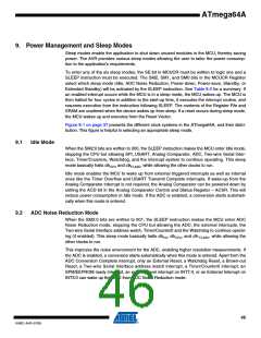
8.10.2
OSCCAL – Oscillator Calibration Register(1)
Bit
7
6
5
4
3
2
1
0
(0x6F)
CAL7
R/W
CAL6
R/W
CAL5
R/W
CAL4
R/W
CAL3
R/W
CAL2
R/W
CAL1
R/W
CAL0
R/W
OSCCAL
Read/Write
Initial Value
Device Specific Calibration Value
Note:
1. The OSCCAL Register is not available in ATmega103 compatibility mode.
• Bits 7:0 – CAL7:0: Oscillator Calibration Value
Writing the calibration byte to this address will trim the internal Oscillator to remove process vari-
ations from the Oscillator frequency. During Reset, the 1 MHz calibration value which is located
in the signature row high byte (address 0x00) is automatically loaded into the OSCCAL Register.
If the internal RC is used at other frequencies, the calibration values must be loaded manually.
This can be done by first reading the signature row by a programmer, and then store the calibra-
tion values in the Flash or EEPROM. Then the value can be read by software and loaded into
the OSCCAL Register. When OSCCAL is zero, the lowest available frequency is chosen. Writing
non-zero values to this register will increase the frequency of the internal Oscillator. Writing
44
8160C–AVR–07/09

 ATMEL [ ATMEL ]