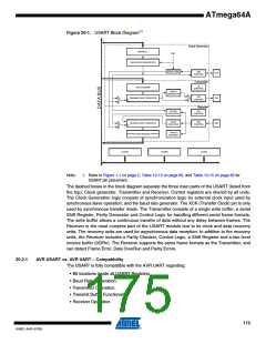
ATmega64A
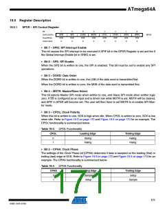
19.5 Register Description
19.5.1
SPCR – SPI Control Register
Bit
7
SPIE
R/W
0
6
5
DORD
R/W
0
4
MSTR
R/W
0
3
CPOL
R/W
0
2
CPHA
R/W
0
1
0
0x0D (0x2D)
Read/Write
Initial Value
SPE
R/W
0
SPR1
R/W
0
SPR0
R/W
0
SPCR
• Bit 7 – SPIE: SPI Interrupt Enable
This bit causes the SPI interrupt to be executed if SPIF bit in the SPSR Register is set and the if
the Global Interrupt Enable bit in SREG is set.
• Bit 6 – SPE: SPI Enable
When the SPE bit is written to one, the SPI is enabled. This bit must be set to enable any SPI
operations.
• Bit 5 – DORD: Data Order
When the DORD bit is written to one, the LSB of the data word is transmitted first.
When the DORD bit is written to zero, the MSB of the data word is transmitted first.
• Bit 4 – MSTR: Master/Slave Select
This bit selects Master SPI mode when written to one, and Slave SPI mode when written logic
zero. If SS is configured as an input and is driven low while MSTR is set, MSTR will be cleared,
and SPIF in SPSR will become set. The user will then have to set MSTR to re-enable SPI Mas-
ter mode.
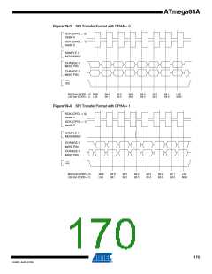
• Bit 3 – CPOL: Clock Polarity
When this bit is written to one, SCK is high when idle. When CPOL is written to zero, SCK is low
when idle. Refer to Figure 19-3 on page 170 and Figure 19-4 on page 170 for an example. The
CPOL functionality is summarized below:
Table 19-3. CPOL Functionality
CPOL
Leading Edge
Rising
Trailing Edge
Falling
0
1
Falling
Rising
• Bit 2 – CPHA: Clock Phase
The settings of the Clock Phase bit (CPHA) determine if data is sampled on the leading (first) or
trailing (last) edge of SCK. Refer to Figure 19-3 on page 170 and Figure 19-4 on page 170 for an
example. The CPHA functionality is summarized below:
Table 19-4. CPHA Functionality
CPHA
Leading Edge
Sample
Trailing Edge
Setup
0
1
Setup
Sample
171
8160C–AVR–07/09

 ATMEL [ ATMEL ]