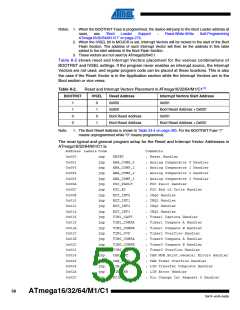
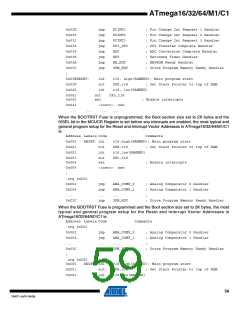
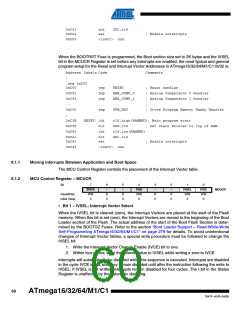
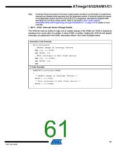
9. I/O-Ports
9.1
Introduction
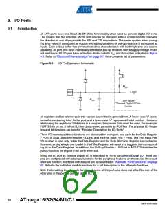
All AVR ports have true Read-Modify-Write functionality when used as general digital I/O ports.
This means that the direction of one port pin can be changed without unintentionally changing
the direction of any other pin with the SBI and CBI instructions. The same applies when chang-
ing drive value (if configured as output) or enabling/disabling of pull-up resistors (if configured as
input). Each output buffer has symmetrical drive characteristics with both high sink and source
capability. All port pins have individually selectable pull-up resistors with a supply-voltage invari-
ant resistance. All I/O pins have protection diodes to both VCC and Ground as indicated in Figure
9-1. Refer to “Electrical Characteristics” on page 317 for a complete list of parameters.
Figure 9-1. I/O Pin Equivalent Schematic
Rpu
Pxn
Logic
Cpin
See Figure
"General Digital I/O" for
Details
All registers and bit references in this section are written in general form. A lower case “x” repre-
sents the numbering letter for the port, and a lower case “n” represents the bit number. However,
when using the register or bit defines in a program, the precise form must be used. For example,
PORTB3 for bit no. 3 in Port B, here documented generally as PORTxn. The physical I/O Regis-
ters and bit locations are listed in “Register Description for I/O-Ports”.
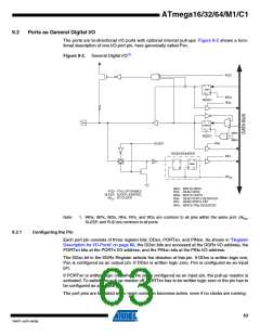
Three I/O memory address locations are allocated for each port, one each for the Data Register
– PORTx, Data Direction Register – DDRx, and the Port Input Pins – PINx. The Port Input Pins
I/O location is read only, while the Data Register and the Data Direction Register are read/write.
However, writing a logic one to a bit in the PINx Register, will result in a toggle in the correspond-
ing bit in the Data Register. In addition, the Pull-up Disable – PUD bit in MCUCR disables the
pull-up function for all pins in all ports when set.
Using the I/O port as General Digital I/O is described in “Ports as General Digital I/O”. Most port
pins are multiplexed with alternate functions for the peripheral features on the device. How each
alternate function interferes with the port pin is described in “Alternate Port Functions” on page
67. Refer to the individual module sections for a full description of the alternate functions.
Note that enabling the alternate function of some of the port pins does not affect the use of the
other pins in the port as general digital I/O.
62
ATmega16/32/64/M1/C1
7647F–AVR–04/09

 ATMEL [ ATMEL ]