ATmega16/32/64/M1/C1
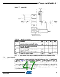
Figure 7-1. Reset Logic
DATA BUS
MCU Status
Register (MCUSR)
Power-on Reset
Circuit
Brown-out
Reset Circuit
BODLEVEL [2..0]
Pull-up Resistor
Spike
Filter
Watchdog
Oscillator
Delay Counters
Clock
Generator
CK
TIMEOUT
CKSEL[3:0]
SUT[1:0]
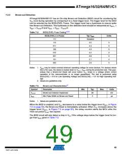
Table 7-1.
Symbol
Reset Characteristics
Parameter
Min
1.1
0.8
Typ
1.4
0.9
Max
Units
Power-on Reset Threshold Voltage (rising)
Power-on Reset Threshold Voltage (falling)(1)
1.7
1.6
V
V
VPOT
VCC Max. start voltage to ensure internal
Power-on Reset signal
VPORMAX
VPORMIN
0.4
V
V
VCC Min. start voltage to ensure internal
Power-on Reset signal
-0.1
VCCRR
VRST
VCC Rise Rate to ensure Power-on Reset
RESET Pin Threshold Voltage
0.01
V/ms
V
0.1 VCC
0.9VCC
Note:
1. Before rising, the supply has to be between VPORMIN and VPORMAX to ensure a Reset.
7.2.1
Power-on Reset
A Power-on Reset (POR) pulse is generated by an On-chip detection circuit. The detection level
is defined in Table 7-1. The POR is activated whenever VCC is below the detection level. The
POR circuit can be used to trigger the start-up Reset, as well as to detect a failure in supply
voltage.
A Power-on Reset (POR) circuit ensures that the device is reset from Power-on. Reaching the
Power-on Reset threshold voltage invokes the delay counter, which determines how long the
device is kept in RESET after VCC rise. The RESET signal is activated again, without any delay,
when VCC decreases below the detection level.
47
7647F–AVR–04/09

 ATMEL [ ATMEL ]