ATmega16/32/64/M1/C1
3.7
Instruction Execution Timing
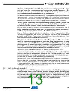
This section describes the general access timing concepts for instruction execution. The AVR
CPU is driven by the CPU clock clkCPU, directly generated from the selected clock source for the
chip. No internal clock division is used.
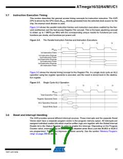
Figure 3-4 shows the parallel instruction fetches and instruction executions enabled by the Har-
vard architecture and the fast-access Register File concept. This is the basic pipelining concept
to obtain up to 1 MIPS per MHz with the corresponding unique results for functions per cost,
functions per clocks, and functions per power-unit.
Figure 3-4. The Parallel Instruction Fetches and Instruction Executions
T1
T2
T3
T4
clkCPU
1st Instruction Fetch
1st Instruction Execute
2nd Instruction Fetch
2nd Instruction Execute
3rd Instruction Fetch
3rd Instruction Execute
4th Instruction Fetch
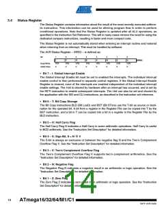
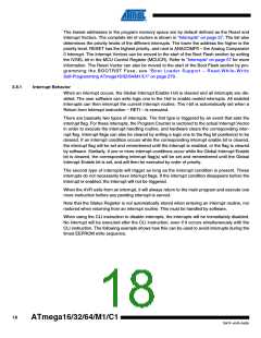
Figure 3-5 shows the internal timing concept for the Register File. In a single clock cycle an ALU
operation using two register operands is executed, and the result is stored back to the destina-
tion register.
Figure 3-5. Single Cycle ALU Operation
T1
T2
T3
T4
clkCPU
Total Execution Time
Register Operands Fetch
ALU Operation Execute
Result Write Back
3.8
Reset and Interrupt Handling
The AVR provides several different interrupt sources. These interrupts and the separate Reset
Vector each have a separate program vector in the program memory space. All interrupts are
assigned individual enable bits which must be written logic one together with the Global Interrupt
Enable bit in the Status Register in order to enable the interrupt. Depending on the Program
Counter value, interrupts may be automatically disabled when Boot Lock bits BLB02 or BLB12
are programmed. This feature improves software security. See the section “Memory Program-
ming” on page 296 for details.
17
7647F–AVR–04/09

 ATMEL [ ATMEL ]