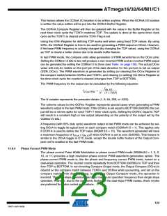
ATmega16/32/64/M1/C1
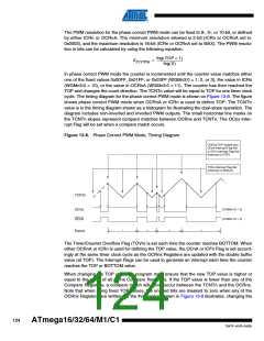
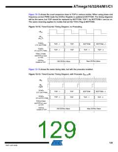
As Figure 13-9 shows the output generated is, in contrast to the phase correct mode, symmetri-
cal in all periods. Since the OCRnx Registers are updated at BOTTOM, the length of the rising
and the falling slopes will always be equal. This gives symmetrical output pulses and is therefore
frequency correct.
Using the ICRn Register for defining TOP works well when using fixed TOP values. By using
ICRn, the OCRnA Register is free to be used for generating a PWM output on OCnA. However,
if the base PWM frequency is actively changed by changing the TOP value, using the OCRnA as
TOP is clearly a better choice due to its double buffer feature.
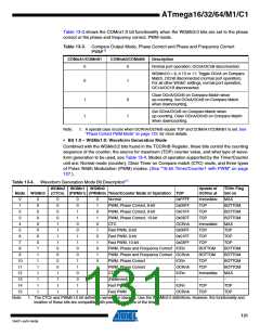
In phase and frequency correct PWM mode, the compare units allow generation of PWM wave-
forms on the OCnx pins. Setting the COMnx1:0 bits to two will produce a non-inverted PWM and
an inverted PWM output can be generated by setting the COMnx1:0 to three (See Table on
page 131). The actual OCnx value will only be visible on the port pin if the data direction for the
port pin is set as output (DDR_OCnx). The PWM waveform is generated by setting (or clearing)
the OCnx Register at the compare match between OCRnx and TCNTn when the counter incre-
ments, and clearing (or setting) the OCnx Register at compare match between OCRnx and
TCNTn when the counter decrements. The PWM frequency for the output when using phase
and frequency correct PWM can be calculated by the following equation:
f
clk_I/O
f
= ---------------------------------
OCnxPFCPWM
2
N
TOP
The N variable represents the prescaler divider (1, 8, 64, 256, or 1024).
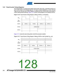
The extreme values for the OCRnx Register represents special cases when generating a PWM
waveform output in the phase correct PWM mode. If the OCRnx is set equal to BOTTOM the
output will be continuously low and if set equal to TOP the output will be set to high for
non-inverted PWM mode. For inverted PWM the output will have the opposite logic values. If
OCR1A is used to define the TOP value (WGM13:0 = 9) and COM1A1:0 = 1, the OC1A output
will toggle with a 50% duty cycle.
127
7647F–AVR–04/09

 ATMEL [ ATMEL ]