ATmega48/88/168
6. Any memory location can be verified by using the Read instruction which returns the con-
tent at the selected address at serial output MISO.
7. At the end of the programming session, RESET can be set high to commence normal
operation.
8. Power-off sequence (if needed):
Set RESET to “1”.
Turn VCC power off.
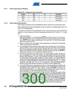
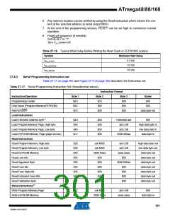
Table 27-16. Typical Wait Delay Before Writing the Next Flash or EEPROM Location
Symbol
Minimum Wait Delay
4.5 ms
tWD_FLASH
tWD_EEPROM
tWD_ERASE
3.6 ms
9.0 ms
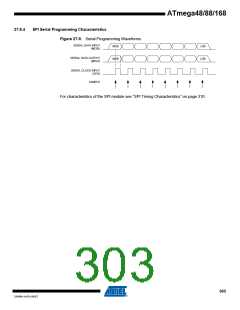
27.8.3
Serial Programming Instruction set
Table 27-17 on page 301 and Figure 27-8 on page 302 describes the Instruction set.
Table 27-17. Serial Programming Instruction Set (Hexadecimal values)
Instruction Format
Instruction/Operation
Byte 1
$AC
Byte 2
Byte 3
$00
Byte4
$00
Programming Enable
$53
$80
$00
Chip Erase (Program Memory/EEPROM)
Poll RDY/BSY
$AC
$00
$00
$F0
$00
data byte out
Load Instructions
Load Extended Address byte(1)
Load Program Memory Page, High byte
Load Program Memory Page, Low byte
Load EEPROM Memory Page (page access)
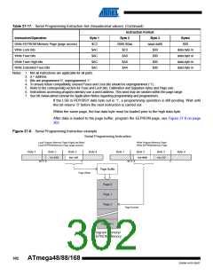
Read Instructions
$4D
$48
$40
$C1
$00
$00
$00
$00
Extended adr
adr LSB
$00
high data byte in
low data byte in
data byte in
adr LSB
0000 000aa
Read Program Memory, High byte
Read Program Memory, Low byte
Read EEPROM Memory
Read Lock bits
$28
$20
$A0
$58
$30
$50
$58
$50
$38
adr MSB
adr MSB
0000 00aa
$00
adr LSB
adr LSB
aaaa aaaa
$00
high data byte out
low data byte out
data byte out
data byte out
data byte out
data byte out
data byte out
data byte out
data byte out
Read Signature Byte
$00
0000 000aa
$00
Read Fuse bits
$00
Read Fuse High bits
$08
$00
Read Extended Fuse Bits
$08
$00
Read Calibration Byte
$00
$00
Write Instructions(6)
Write Program Memory Page
Write EEPROM Memory
$4C
$C0
adr MSB
adr LSB
$00
0000 00aa
aaaa aaaa
data byte in
301
2545M–AVR–09/07

 ATMEL [ ATMEL ]