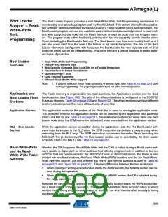
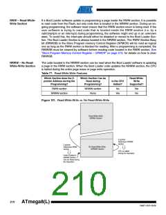
ATmega8(L)
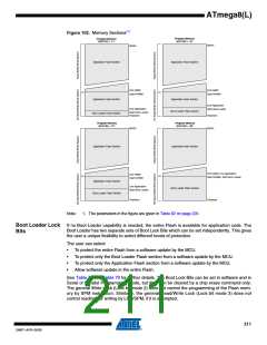
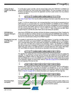
Table 80. Boot Reset Fuse(1)
BOOTRST
Reset Address
1
0
Reset Vector = Application Reset (address 0x0000)
Reset Vector = Boot Loader Reset (see Table 82 on page 220)
Note:
1. “1” means unprogrammed, “0” means programmed
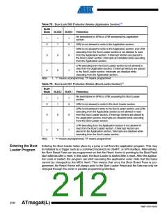
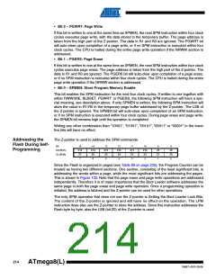
Store Program
Memory Control
Register – SPMCR
The Store Program memory Control Register contains the control bits needed to control the Boot
Loader operations.
Bit
7
SPMIE
R/W
0
6
5
–
4
RWWSRE
R/W
3
BLBSET
R/W
0
2
PGWRT
R/W
0
1
PGERS
R/W
0
0
SPMEN
R/W
0
RWWSB
SPMCR
Read/Write
Initial Value
R
0
R
0
0
• Bit 7 – SPMIE: SPM Interrupt Enable
When the SPMIE bit is written to one, and the I-bit in the Status Register is set (one), the SPM
ready interrupt will be enabled. The SPM ready Interrupt will be executed as long as the SPMEN
bit in the SPMCR Register is cleared.
• Bit 6 – RWWSB: Read-While-Write Section Busy
When a Self-Programming (page erase or page write) operation to the RWW section is initiated,
the RWWSB will be set (one) by hardware. When the RWWSB bit is set, the RWW section can-
not be accessed. The RWWSB bit will be cleared if the RWWSRE bit is written to one after a
Self-Programming operation is completed. Alternatively the RWWSB bit will automatically be
cleared if a page load operation is initiated.
• Bit 5 – Res: Reserved Bit
This bit is a reserved bit in the ATmega8 and always read as zero.
• Bit 4 – RWWSRE: Read-While-Write Section Read Enable
When programming (page erase or page write) to the RWW section, the RWW section is
blocked for reading (the RWWSB will be set by hardware). To re-enable the RWW section, the
user software must wait until the programming is completed (SPMEN will be cleared). Then, if
the RWWSRE bit is written to one at the same time as SPMEN, the next SPM instruction within
four clock cycles re-enables the RWW section. The RWW section cannot be re-enabled while
the Flash is busy with a page erase or a page write (SPMEN is set). If the RWWSRE bit is writ-
ten while the Flash is being loaded, the Flash load operation will abort and the data loaded will
be lost (The page buffer will be cleared when the Read-While-Write section is re-enabled).
• Bit 3 – BLBSET: Boot Lock Bit Set
If this bit is written to one at the same time as SPMEN, the next SPM instruction within four clock
cycles sets Boot Lock Bits, according to the data in R0. The data in R1 and the address in the Z-
pointer are ignored. The BLBSET bit will automatically be cleared upon completion of the lock bit
set, or if no SPM instruction is executed within four clock cycles.
An LPM instruction within three cycles after BLBSET and SPMEN are set in the SPMCR Regis-
ter, will read either the Lock Bits or the Fuse Bits (depending on Z0 in the Z-pointer) into the
destination register. See “Reading the Fuse and Lock Bits from Software” on page 217 for
details.
213
2486T–AVR–05/08

 ATMEL [ ATMEL ]