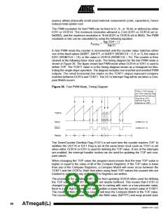
update of the OCR1x Compare Register to either TOP or BOTTOM of the counting
sequence. The synchronization prevents the occurrence of odd-length, non-symmetrical
PWM pulses, thereby making the output glitch-free.
The OCR1x Register access may seem complex, but this is not case. When the double
buffering is enabled, the CPU has access to the OCR1x Buffer Register, and if double
buffering is disabled the CPU will access the OCR1x directly. The content of the OCR1x
(Buffer or Compare) Register is only changed by a write operation (the Timer/Counter
does not update this register automatically as the TCNT1 and ICR1 Register). Therefore
OCR1x is not read via the High byte temporary register (TEMP). However, it is a good
practice to read the Low byte first as when accessing other 16-bit registers. Writing the
OCR1x Registers must be done via the TEMP Register since the compare of all 16-bit is
done continuously. The High byte (OCR1xH) has to be written first. When the High byte
I/O location is written by the CPU, the TEMP Register will be updated by the value writ-
ten. Then when the Low byte (OCR1xL) is written to the lower eight bits, the High byte
will be copied into the upper 8-bits of either the OCR1x buffer or OCR1x Compare Reg-
ister in the same system clock cycle.
For more information of how to access the 16-bit registers refer to “Accessing 16-bit
Registers” on page 77.
Force Output Compare
In non-PWM Waveform Generation modes, the match output of the comparator can be
forced by writing a one to the Force Output Compare (FOC1x) bit. Forcing Compare
Match will not set the OCF1x Flag or reload/clear the timer, but the OC1x pin will be
updated as if a real Compare Match had occurred (the COM1x1:0 bits settings define
whether the OC1x pin is set, cleared or toggled).
Compare Match Blocking by
TCNT1 Write
All CPU writes to the TCNT1 Register will block any Compare Match that occurs in the
next timer clock cycle, even when the timer is stopped. This feature allows OCR1x to be
initialized to the same value as TCNT1 without triggering an interrupt when the
Timer/Counter clock is enabled.
Using the Output Compare
Unit
Since writing TCNT1 in any mode of operation will block all compare matches for one
timer clock cycle, there are risks involved when changing TCNT1 when using any of the
Output Compare channels, independent of whether the Timer/Counter is running or not.
If the value written to TCNT1 equals the OCR1x value, the Compare Match will be
missed, resulting in incorrect waveform generation. Do not write the TCNT1 equal to
TOP in PWM modes with variable TOP values. The Compare Match for the TOP will be
ignored and the counter will continue to 0xFFFF. Similarly, do not write the TCNT1 value
equal to BOTTOM when the counter is downcounting.
The setup of the OC1x should be performed before setting the Data Direction Register
for the port pin to output. The easiest way of setting the OC1x value is to use the Force
Output Compare (FOC1x) strobe bits in Normal mode. The OC1x Register keeps its
value even when changing between Waveform Generation modes.
Be aware that the COM1x1:0 bits are not double buffered together with the compare
value. Changing the COM1x1:0 bits will take effect immediately.
84
ATmega8(L)
2486M–AVR–12/03

 ATMEL [ ATMEL ]