ATmega8(L)
inverting Oscillator amplifier. In this mode, a crystal Oscillator is connected to this pin,
and the pin can not be used as an I/O pin.
If PB6 is used as a clock pin, DDB6, PORTB6 and PINB6 will all read 0.
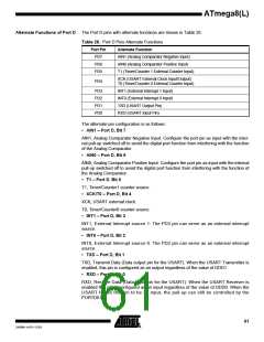
• SCK – Port B, Bit 5
SCK: Master Clock output, Slave Clock input pin for SPI channel. When the SPI is
enabled as a Slave, this pin is configured as an input regardless of the setting of DDB5.
When the SPI is enabled as a Master, the data direction of this pin is controlled by
DDB5. When the pin is forced by the SPI to be an input, the pull-up can still be con-
trolled by the PORTB5 bit.
• MISO – Port B, Bit 4
MISO: Master Data input, Slave Data output pin for SPI channel. When the SPI is
enabled as a Master, this pin is configured as an input regardless of the setting of
DDB4. When the SPI is enabled as a Slave, the data direction of this pin is controlled by
DDB4. When the pin is forced by the SPI to be an input, the pull-up can still be con-
trolled by the PORTB4 bit.
• MOSI/OC2 – Port B, Bit 3
MOSI: SPI Master Data output, Slave Data input for SPI channel. When the SPI is
enabled as a Slave, this pin is configured as an input regardless of the setting of DDB3.
When the SPI is enabled as a Master, the data direction of this pin is controlled by
DDB3. When the pin is forced by the SPI to be an input, the pull-up can still be con-
trolled by the PORTB3 bit.
OC2, Output Compare Match Output: The PB3 pin can serve as an external output for
the Timer/Counter2 Compare Match. The PB3 pin has to be configured as an output
(DDB3 set (one)) to serve this function. The OC2 pin is also the output pin for the PWM
mode timer function.
• SS/OC1B – Port B, Bit 2
SS: Slave Select input. When the SPI is enabled as a Slave, this pin is configured as an
input regardless of the setting of DDB2. As a Slave, the SPI is activated when this pin is
driven low. When the SPI is enabled as a Master, the data direction of this pin is con-
trolled by DDB2. When the pin is forced by the SPI to be an input, the pull-up can still be
controlled by the PORTB2 bit.
OC1B, Output Compare Match output: The PB2 pin can serve as an external output for
the Timer/Counter1 Compare Match B. The PB2 pin has to be configured as an output
(DDB2 set (one)) to serve this function. The OC1B pin is also the output pin for the PWM
mode timer function.
• OC1A – Port B, Bit 1
OC1A, Output Compare Match output: The PB1 pin can serve as an external output for
the Timer/Counter1 Compare Match A. The PB1 pin has to be configured as an output
(DDB1 set (one)) to serve this function. The OC1A pin is also the output pin for the PWM
mode timer function.
• ICP1 – Port B, Bit 0
ICP1 – Input Capture Pin: The PB0 pin can act as an Input Capture Pin for
Timer/Counter1.
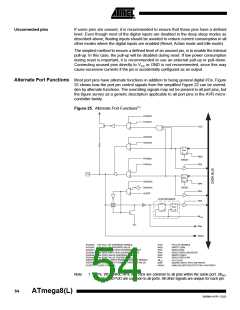
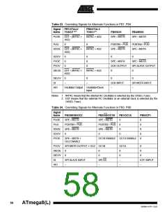
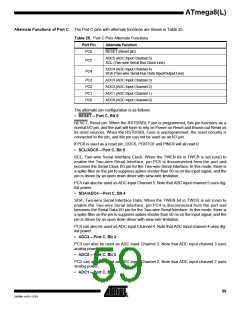
Table 23 and Table 24 relate the alternate functions of Port B to the overriding signals
shown in Figure 25 on page 54. SPI MSTR INPUT and SPI SLAVE OUTPUT constitute
the MISO signal, while MOSI is divided into SPI MSTR OUTPUT and SPI SLAVE
INPUT.
57
2486M–AVR–12/03

 ATMEL [ ATMEL ]