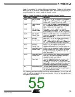
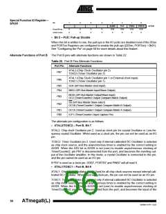
Special Function IO Register –
SFIOR
Bit
7
6
5
4
3
ACME
R/W
0
2
1
PSR2
R/W
0
0
PSR10
R/W
0
PUD
R/W
0
SFIOR
Read/Write
Initial Value
R
0
R
0
R
0
R
0
• Bit 2 – PUD: Pull-up Disable
When this bit is written to one, the pull-ups in the I/O ports are disabled even if the DDxn
and PORTxn Registers are configured to enable the pull-ups ({DDxn, PORTxn} = 0b01).
See “Configuring the Pin” on page 50 for more details about this feature.
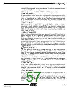
Alternate Functions of Port B The Port B pins with alternate functions are shown in Table 22.
Table 22. Port B Pins Alternate Functions
Port Pin
Alternate Functions
XTAL2 (Chip Clock Oscillator pin 2)
TOSC2 (Timer Oscillator pin 2)
PB7
XTAL1 (Chip Clock Oscillator pin 1 or External clock input)
TOSC1 (Timer Oscillator pin 1)
PB6
PB5
PB4
SCK (SPI Bus Master clock Input)
MISO (SPI Bus Master Input/Slave Output)
MOSI (SPI Bus Master Output/Slave Input)
OC2 (Timer/Counter2 Output Compare Match Output)
PB3
PB2
SS (SPI Bus Master Slave select)
OC1B (Timer/Counter1 Output Compare Match B Output)
PB1
PB0
OC1A (Timer/Counter1 Output Compare Match A Output)
ICP1 (Timer/Counter1 Input Capture Pin)
The alternate pin configuration is as follows:
• XTAL2/TOSC2 – Port B, Bit 7
XTAL2: Chip clock Oscillator pin 2. Used as clock pin for crystal Oscillator or Low-fre-
quency crystal Oscillator. When used as a clock pin, the pin can not be used as an I/O
pin.
TOSC2: Timer Oscillator pin 2. Used only if internal calibrated RC Oscillator is selected
as chip clock source, and the asynchronous timer is enabled by the correct setting in
ASSR. When the AS2 bit in ASSR is set (one) to enable asynchronous clocking of
Timer/Counter2, pin PB7 is disconnected from the port, and becomes the inverting out-
put of the Oscillator amplifier. In this mode, a crystal Oscillator is connected to this pin,
and the pin cannot be used as an I/O pin.
If PB7 is used as a clock pin, DDB7, PORTB7 and PINB7 will all read 0.
• XTAL1/TOSC1 – Port B, Bit 6
XTAL1: Chip clock Oscillator pin 1. Used for all chip clock sources except internal cali-
brated RC Oscillator. When used as a clock pin, the pin can not be used as an I/O pin.
TOSC1: Timer Oscillator pin 1. Used only if internal calibrated RC Oscillator is selected
as chip clock source, and the asynchronous timer is enabled by the correct setting in
ASSR. When the AS2 bit in ASSR is set (one) to enable asynchronous clocking of
Timer/Counter2, pin PB6 is disconnected from the port, and becomes the input of the
56
ATmega8(L)
2486M–AVR–12/03

 ATMEL [ ATMEL ]