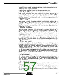
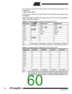
ATmega8(L)
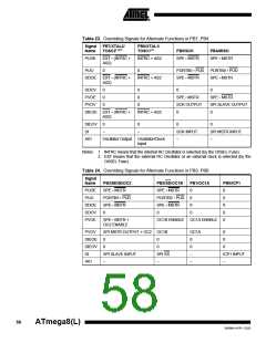
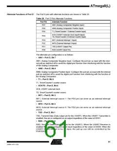
Alternate Functions of Port D The Port D pins with alternate functions are shown in Table 28.
Table 28. Port D Pins Alternate Functions
Port Pin
PD7
Alternate Function
AIN1 (Analog Comparator Negative Input)
AIN0 (Analog Comparator Positive Input)
T1 (Timer/Counter 1 External Counter Input)
PD6
PD5
XCK (USART External Clock Input/Output)
T0 (Timer/Counter 0 External Counter Input)
PD4
PD3
PD2
PD1
PD0
INT1 (External Interrupt 1 Input)
INT0 (External Interrupt 0 Input)
TXD (USART Output Pin)
RXD (USART Input Pin)
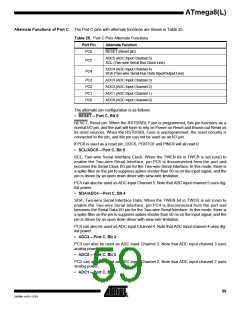
The alternate pin configuration is as follows:
• AIN1 – Port D, Bit 7
AIN1, Analog Comparator Negative Input. Configure the port pin as input with the inter-
nal pull-up switched off to avoid the digital port function from interfering with the function
of the Analog Comparator.
• AIN0 – Port D, Bit 6
AIN0, Analog Comparator Positive Input. Configure the port pin as input with the internal
pull-up switched off to avoid the digital port function from interfering with the function of
the Analog Comparator.
• T1 – Port D, Bit 5
T1, Timer/Counter1 counter source.
• XCK/T0 – Port D, Bit 4
XCK, USART external clock.
T0, Timer/Counter0 counter source.
• INT1 – Port D, Bit 3
INT1, External Interrupt source 1: The PD3 pin can serve as an external interrupt
source.
• INT0 – Port D, Bit 2
INT0, External Interrupt source 0: The PD2 pin can serve as an external interrupt
source.
• TXD – Port D, Bit 1
TXD, Transmit Data (Data output pin for the USART). When the USART Transmitter is
enabled, this pin is configured as an output regardless of the value of DDD1.
• RXD – Port D, Bit 0
RXD, Receive Data (Data input pin for the USART). When the USART Receiver is
enabled this pin is configured as an input regardless of the value of DDD0. When the
USART forces this pin to be an input, the pull-up can still be controlled by the
PORTD0 bit.
61
2486M–AVR–12/03

 ATMEL [ ATMEL ]