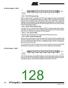
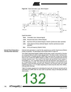
Figure 62. Clock Generation Logic, Block Diagram
UBRR
U2X
fosc
UBRR+1
Prescaling
Down-Counter
/ 2
/ 4
/ 2
0
1
0
1
OSC
txclk
UMSEL
rxclk
DDR_XCK
Sync
Register
Edge
Detector
xcki
0
1
XCK
Pin
xcko
DDR_XCK
UCPOL
1
0
Signal description:
txclk Transmitter clock. (Internal Signal)
rxclk Receiver base clock. (Internal Signal)
xcki
Input from XCK pin (internal Signal). Used for synchronous slave operation.
xcko Clock output to XCK pin (Internal Signal). Used for synchronous master
operation.
fosc
XTAL pin frequency (System Clock).
Internal Clock Generation –
The Baud Rate Generator
Internal clock generation is used for the asynchronous and the Synchronous Master
modes of operation. The description in this section refers to Figure 62.
The USART Baud Rate Register (UBRR) and the down-counter connected to it function
as a programmable prescaler or baud rate generator. The down-counter, running at sys-
tem clock (fosc), is loaded with the UBRR value each time the counter has counted
down to zero or when the UBRRL Register is written. A clock is generated each time the
counter reaches zero. This clock is the baud rate generator clock output (=
fosc/(UBRR+1)). The Transmitter divides the baud rate generator clock output by 2, 8,
or 16 depending on mode. The baud rate generator output is used directly by the
Receiver’s clock and data recovery units. However, the recovery units use a state
machine that uses 2, 8, or 16 states depending on mode set by the state of the UMSEL,
U2X and DDR_XCK bits.
Table 52 contains equations for calculating the baud rate (in bits per second) and for
calculating the UBRR value for each mode of operation using an internally generated
clock source.
132
ATmega8(L)
2486M–AVR–12/03

 ATMEL [ ATMEL ]