ATmega8(L)
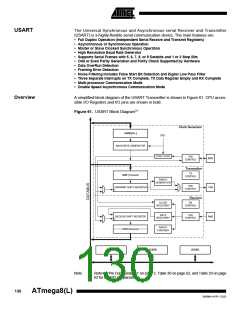
The dashed boxes in the block diagram separate the three main parts of the USART
(listed from the top): Clock generator, Transmitter and Receiver. Control Registers are
shared by all units. The clock generation logic consists of synchronization logic for exter-
nal clock input used by synchronous slave operation, and the baud rate generator. The
XCK (transfer clock) pin is only used by synchronous transfer mode. The Transmitter
consists of a single write buffer, a serial Shift Register, Parity Generator and control
logic for handling different serial frame formats. The write buffer allows a continuous
transfer of data without any delay between frames. The Receiver is the most complex
part of the USART module due to its clock and data recovery units. The recovery units
are used for asynchronous data reception. In addition to the recovery units, the Receiver
includes a parity checker, control logic, a Shift Register and a two level receive buffer
(UDR). The Receiver supports the same frame formats as the Transmitter, and can
detect Frame Error, Data OverRun and Parity Errors.
AVR USART vs. AVR UART –
Compatibility
The USART is fully compatible with the AVR UART regarding:
•
•
•
•
•
Bit locations inside all USART Registers.
Baud Rate Generation.
Transmitter Operation.
Transmit Buffer Functionality.
Receiver Operation.
However, the receive buffering has two improvements that will affect the compatibility in
some special cases:
•
A second Buffer Register has been added. The two Buffer Registers operate as a
circular FIFO buffer. Therefore the UDR must only be read once for each incoming
data! More important is the fact that the Error Flags (FE and DOR) and the ninth
data bit (RXB8) are buffered with the data in the receive buffer. Therefore the status
bits must always be read before the UDR Register is read. Otherwise the error
status will be lost since the buffer state is lost.
•
The Receiver Shift Register can now act as a third buffer level. This is done by
allowing the received data to remain in the serial Shift Register (see Figure 61) if the
Buffer Registers are full, until a new start bit is detected. The USART is therefore
more resistant to Data OverRun (DOR) error conditions.
The following control bits have changed name, but have same functionality and register
location:
•
•
CHR9 is changed to UCSZ2.
OR is changed to DOR.
Clock Generation
The clock generation logic generates the base clock for the Transmitter and Receiver.
The USART supports four modes of clock operation: normal asynchronous, double
speed asynchronous, Master synchronous and Slave Synchronous mode. The UMSEL
bit in USART Control and Status Register C (UCSRC) selects between asynchronous
and synchronous operation. Double speed (Asynchronous mode only) is controlled by
the U2X found in the UCSRA Register. When using Synchronous mode (UMSEL = 1),
the Data Direction Register for the XCK pin (DDR_XCK) controls whether the clock
source is internal (Master mode) or external (Slave mode). The XCK pin is only active
when using Synchronous mode.
Figure 62 shows a block diagram of the clock generation logic.
131
2486M–AVR–12/03

 ATMEL [ ATMEL ]