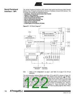
Serial Peripheral
Interface – SPI
The Serial Peripheral Interface (SPI) allows high-speed synchronous data transfer
between the ATmega8 and peripheral devices or between several AVR devices. The
ATmega8 SPI includes the following features:
• Full-duplex, Three-wire Synchronous Data Transfer
• Master or Slave Operation
• LSB First or MSB First Data Transfer
• Seven Programmable Bit Rates
• End of Transmission Interrupt Flag
• Write Collision Flag Protection
• Wake-up from Idle Mode
• Double Speed (CK/2) Master SPI Mode
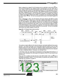
Figure 57. SPI Block Diagram(1)
DIVIDER
/2/4/8/16/32/64/128
Note:
1. Refer to “Pin Configurations” on page 2, and Table 22 on page 56 for SPI pin
placement.
The interconnection between Master and Slave CPUs with SPI is shown in Figure 58.
The system consists of two Shift Registers, and a Master clock generator. The SPI Mas-
ter initiates the communication cycle when pulling low the Slave Select SS pin of the
desired Slave. Master and Slave prepare the data to be sent in their respective Shift
Registers, and the Master generates the required clock pulses on the SCK line to inter-
change data. Data is always shifted from Master to Slave on the Master Out – Slave In,
MOSI, line, and from Slave to Master on the Master In – Slave Out, MISO, line. After
each data packet, the Master will synchronize the Slave by pulling high the Slave Select,
SS, line.
122
ATmega8(L)
2486M–AVR–12/03

 ATMEL [ ATMEL ]