ATmega8(L)
Compare Match Output
Unit
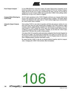
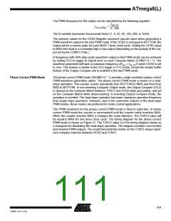
The Compare Output mode (COM21:0) bits have two functions. The waveform genera-
tor uses the COM21:0 bits for defining the Output Compare (OC2) state at the next
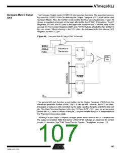
Compare Match. Also, the COM21:0 bits control the OC2 pin output source. Figure 48
shows a simplified schematic of the logic affected by the COM21:0 bit setting. The I/O
Registers, I/O bits, and I/O pins in the figure are shown in bold. Only the parts of the
general I/O Port Control Registers (DDR and PORT) that are affected by the COM21:0
bits are shown. When referring to the OC2 state, the reference is for the internal OC2
Register, not the OC2 pin.
Figure 48. Compare Match Output Unit, Schematic
COMn1
Waveform
Generator
COMn0
FOCn
D
Q
Q
1
0
OCn
Pin
OCn
D
PORT
D
Q
DDR
clkI/O
The general I/O port function is overridden by the Output Compare (OC2) from the
waveform generator if either of the COM21:0 bits are set. However, the OC2 pin direc-
tion (input or output) is still controlled by the Data Direction Register (DDR) for the port
pin. The Data Direction Register bit for the OC2 pin (DDR_OC2) must be set as output
before the OC2 value is visible on the pin. The port override function is independent of
the Waveform Generation mode.
The design of the Output Compare Pin logic allows initialization of the OC2 state before
the output is enabled. Note that some COM21:0 bit settings are reserved for certain
modes of operation. See “8-bit Timer/Counter Register Description” on page 115.
107
2486M–AVR–12/03

 ATMEL [ ATMEL ]