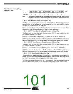
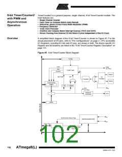
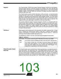
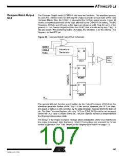
ATmega8(L)
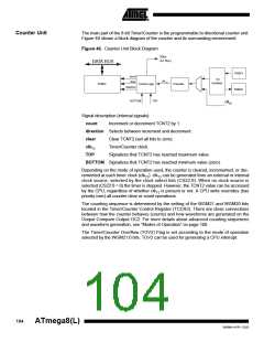
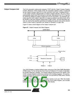
Output Compare Unit
The 8-bit comparator continuously compares TCNT2 with the Output Compare Register
(OCR2). Whenever TCNT2 equals OCR2, the comparator signals a match. A match will
set the Output Compare Flag (OCF2) at the next timer clock cycle. If enabled (OCIE2 =
1), the Output Compare Flag generates an Output Compare interrupt. The OCF2 Flag is
automatically cleared when the interrupt is executed. Alternatively, the OCF2 Flag can
be cleared by software by writing a logical one to its I/O bit location. The waveform gen-
erator uses the match signal to generate an output according to operating mode set by
the WGM21:0 bits and Compare Output mode (COM21:0) bits. The max and bottom sig-
nals are used by the waveform generator for handling the special cases of the extreme
values in some modes of operation (see “Modes of Operation” on page 108).
Figure 47 shows a block diagram of the Output Compare unit.
Figure 47. Output Compare Unit, Block Diagram
DATA BUS
OCRn
TCNTn
= (8-bit Comparator )
OCFn (Int. Req.)
TOP
BOTTOM
FOCn
Waveform Generator
OCxy
WGMn1:0
COMn1:0
The OCR2 Register is double buffered when using any of the Pulse Width Modulation
(PWM) modes. For the normal and Clear Timer on Compare (CTC) modes of operation,
the double buffering is disabled. The double buffering synchronizes the update of the
OCR2 Compare Register to either top or bottom of the counting sequence. The synchro-
nization prevents the occurrence of odd-length, non-symmetrical PWM pulses, thereby
making the output glitch-free.
The OCR2 Register access may seem complex, but this is not case. When the double
buffering is enabled, the CPU has access to the OCR2 Buffer Register, and if double
buffering is disabled the CPU will access the OCR2 directly.
105
2486M–AVR–12/03

 ATMEL [ ATMEL ]