ATmega8(L)
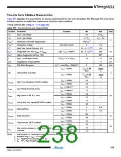
Two-wire Serial Interface Characteristics
Table 101 describes the requirements for devices connected to the Two-wire Serial Bus. The ATmega8 Two-wire Serial
Interface meets or exceeds these requirements under the noted conditions.
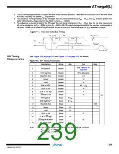
Timing symbols refer to Figure 115 on page 239.
Table 101. Two-wire Serial Bus Requirements
Symbol Parameter
Condition
Min
-0.5
Max
0.3VCC
VCC + 0.5
–
Units
VIL
Input Low-voltage
VIH
Vhys
Input High-voltage
0.7VCC
V
(1)
(1)
(2)
Hysteresis of Schmitt Trigger Inputs
Output Low-voltage
0.05VCC
VOL
tr(1)
3mA sink Current
10pF < Cb < 400pF(3)
0.1VCC < Vi < 0.9VCC
0
0.4
(3)(2)
(3)(2)
Rise Time for both SDA and SCL
Output Fall Time from VIHmin to VILmax
Spikes Suppressed by Input Filter
Input Current each I/O Pin
Capacitance for each I/O Pin
SCL Clock Frequency
20 + 0.1Cb
300
(1)
tof
20 + 0.1Cb
250
ns
tSP
Ii
Ci(1)
fSCL
0
-10
–
50(2)
(1)
10
µA
pF
10
fCK(4) > max(16fSCL, 250kHz)(5)
0
400
kHz
VCC – 0.4V
----------------------------
3mA
fSCL 100kHz
1000ns
Cb
-------------------
Rp
Value of Pull-up resistor
VCC – 0.4V
----------------------------
3mA
fSCL > 100kHz
300ns
---------------
Cb
fSCL 100kHz
fSCL > 100kHz
fSCL 100kHz(6)
4.0
0.6
4.7
1.3
4.0
0.6
4.7
0.6
0
–
tHD;STA
Hold Time (repeated) START Condition
Low Period of the SCL Clock
High period of the SCL clock
Set-up time for a repeated START condition
Data hold time
–
–
tLOW
f
SCL > 100kHz(7)
fSCL 100kHz
fSCL > 100kHz
fSCL 100kHz
fSCL > 100kHz
fSCL 100kHz
–
–
tHIGH
µs
–
–
tSU;STA
tHD;DAT
tSU;DAT
tSU;STO
tBUF
–
3.45
0.9
–
fSCL > 100kHz
0
fSCL 100kHz
fSCL > 100kHz
fSCL 100kHz
250
100
4.0
0.6
4.7
1.3
Data setup time
ns
µs
–
–
Setup time for STOP condition
fSCL > 100kHz
–
fSCL 100kHz
–
Bus free time between a STOP and START
condition
fSCL > 100kHz
–
Notes: 1. In ATmega8, this parameter is characterized and not 100ꢀ tested
2. Required only for fSCL > 100kHz
3. Cb = capacitance of one bus line in pF
4. fCK = CPU clock frequency
238
2486AA–AVR–02/2013

 ATMEL [ ATMEL ]