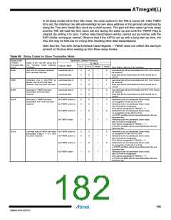
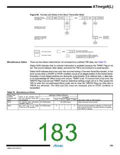
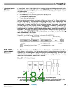
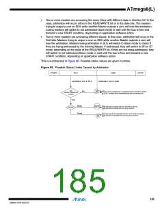
ATmega8(L)
Analog
Comparator
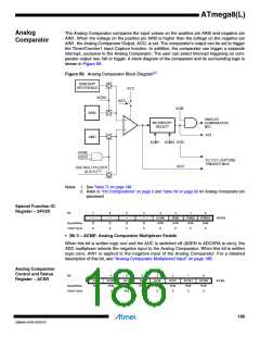
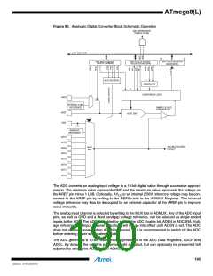
The Analog Comparator compares the input values on the positive pin AIN0 and negative pin
AIN1. When the voltage on the positive pin AIN0 is higher than the voltage on the negative pin
AIN1, the Analog Comparator Output, ACO, is set. The comparator’s output can be set to trigger
the Timer/Counter1 Input Capture function. In addition, the comparator can trigger a separate
interrupt, exclusive to the Analog Comparator. The user can select Interrupt triggering on com-
parator output rise, fall or toggle. A block diagram of the comparator and its surrounding logic is
shown in Figure 89.
Figure 89. Analog Comparator Block Diagram(2)
BANDGAP
REFERENCE
ACBG
ACME
ADEN
ADC MULTIPLEXER
OUTPUT(1)
Notes: 1. See Table 72 on page 188
2. Refer to “Pin Configurations” on page 2 and Table 28 on page 63 for Analog Comparator pin
placement
Special Function IO
Register – SFIOR
Bit
7
–
6
–
5
–
4
–
3
ACME
R/W
0
2
1
PSR2
R/W
0
0
PSR10
R/W
0
PUD
R/W
0
SFIOR
Read/Write
Initial Value
R
0
R
0
R
0
R
0
• Bit 3 – ACME: Analog Comparator Multiplexer Enable
When this bit is written logic one and the ADC is switched off (ADEN in ADCSRA is zero), the
ADC multiplexer selects the negative input to the Analog Comparator. When this bit is written
logic zero, AIN1 is applied to the negative input of the Analog Comparator. For a detailed
description of this bit, see “Analog Comparator Multiplexed Input” on page 188.
Analog Comparator
Control and Status
Register – ACSR
Bit
7
6
ACBG
R/W
0
5
ACO
R
4
ACI
R/W
0
3
ACIE
R/W
0
2
ACIC
R/W
0
1
ACIS1
R/W
0
0
ACIS0
R/W
0
ACD
R/W
0
ACSR
Read/Write
Initial Value
N/A
186
2486AA–AVR–02/2013

 ATMEL [ ATMEL ]