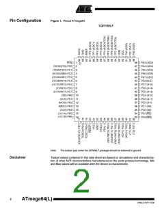
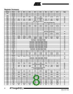
Pin Configuration
Figure 1. Pinout ATmega64
TQFP/MLF
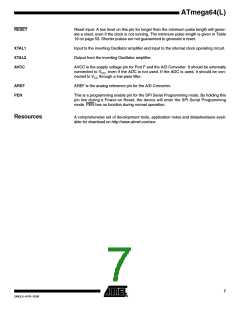
PEN
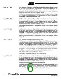
RXD0/(PDI) PE0
(TXD0/PDO) PE1
(XCK0/AIN0) PE2
(OC3A/AIN1) PE3
(OC3B/INT4) PE4
(OC3C/INT5) PE5
(T3/INT6) PE6
1
2
3
4
5
6
7
8
9
48 PA3 (AD3)
47 PA4 (AD4)
46 PA5 (AD5)
45 PA6 (AD6)
44 PA7 (AD7)
43 PG2(ALE)
42 PC7 (A15)
41 PC6 (A14)
40 PC5 (A13)
39 PC4 (A12)
38 PC3 (A11)
37 PC2 (A10
36 PC1 (A9)
35 PC0 (A8)
34 PG1(RD)
33 PG0(WR)
(ICP3/INT7) PE7
(SS) PB0 10
(SCK) PB1 11
(MOSI) PB2 12
(MISO) PB3 13
(OC0) PB4 14
(OC1A) PB5 15
(OC1B) PB6
16
Note:
The bottom pad under the QFN/MLF package should be soldered to ground.
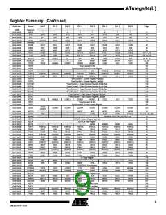
Disclaimer
Typical values contained in this data sheet are based on simulations and characteriza-
tion of other AVR microcontrollers manufactured on the same process technology. Min
and Max values will be available after the device is characterized.
2
ATmega64(L)
2490LS–AVR–10/06

 ATMEL [ ATMEL ]