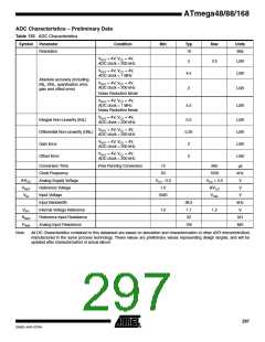
ATmega48/88/168
Typical
Characteristics –
Preliminary Data
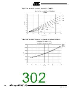
The following charts show typical behavior. These figures are not tested during manu-
facturing. All current consumption measurements are performed with all I/O pins
configured as inputs and with internal pull-ups enabled. A sine wave generator with rail-
to-rail output is used as clock source.
All Active- and Idle current consumption measurements are done with all bits in the PRR
register set and thus, the corresponding I/O modules are turned off. Also the Analog
Comparator is disabled during these measurements. Table 136 on page 304 and Table
137 on page 304 show the additional current consumption compared to ICC Active and
I
CC Idle for every I/O module controlled by the Power Reduction Register. See “Power
Reduction Register” on page 37 for details.
The power consumption in Power-down mode is independent of clock selection.
The current consumption is a function of several factors such as: operating voltage,
operating frequency, loading of I/O pins, switching rate of I/O pins, code executed and
ambient temperature. The dominating factors are operating voltage and frequency.
The current drawn from capacitive loaded pins may be estimated (for one pin) as
CL*VCC*f where CL = load capacitance, VCC = operating voltage and f = average switch-
ing frequency of I/O pin.
The parts are characterized at frequencies higher than test limits. Parts are not guaran-
teed to function properly at frequencies higher than the ordering code indicates.
The difference between current consumption in Power-down mode with Watchdog
Timer enabled and Power-down mode with Watchdog Timer disabled represents the dif-
ferential current drawn by the Watchdog Timer.
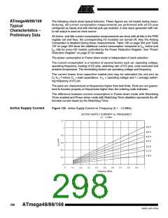
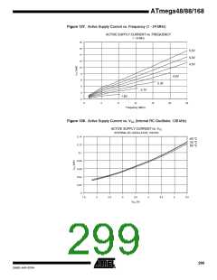
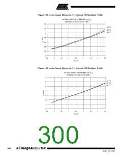
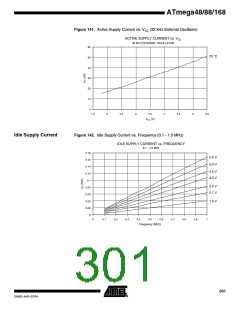
Active Supply Current
Figure 136. Active Supply Current vs. Frequency (0.1 - 1.0 MHz)
ACTIVE SUPPLY CURRENT vs. FREQUENCY
0.1 - 1.0 MHz
1.2
5.5 V
1
5.0 V
0.8
4.5 V
4.0 V
0.6
3.3 V
0.4
2.7 V
1.8 V
0.2
0
0
0.1
0.2
0.3
0.4
0.5
0.6
0.7
0.8
0.9
1
Frequency (MHz)
298
ATmega48/88/168
2545D–AVR–07/04

 ATMEL [ ATMEL ]