When programming the EEPROM, an auto-erase cycle is built into the self-timed pro-
gramming operation (in the Serial mode ONLY) and there is no need to first execute the
Chip Erase instruction. The Chip Erase operation turns the content of every memory
location in both the Program and EEPROM arrays into 0xFF.
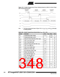
Depending on CKSEL Fuses, a valid clock must be present. The minimum low and high
periods for the serial clock (SCK) input are defined as follows:
Low:> 2 CPU clock cycles for fck < 12 MHz, 3 CPU clock cycles for fck >= 12 MHz
High:> 2 CPU clock cycles for fck < 12 MHz, 3 CPU clock cycles for fck >= 12 MHz
Serial Programming
Algorithm
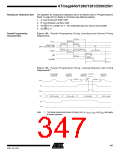
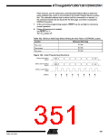
When writing serial data to the ATmega640/1280/1281/2560/2561, data is clocked on
the rising edge of SCK.
When reading data from the ATmega640/1280/1281/2560/2561, data is clocked on the
falling edge of SCK. See Figure 149 for timing details.
To program and verify the ATmega640/1280/1281/2560/2561 in the serial programming
mode, the following sequence is recommended (See four byte instruction formats in
Table 163):
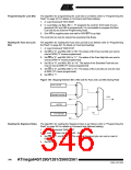
1. Power-up sequence:
Apply power between VCC and GND while RESET and SCK are set to “0”. In
some systems, the programmer can not guarantee that SCK is held low during
power-up. In this case, RESET must be given a positive pulse of at least two
CPU clock cycles duration after SCK has been set to “0”.
2. Wait for at least 20 ms and enable serial programming by sending the Program-
ming Enable serial instruction to pin PDI.
3. The serial programming instructions will not work if the communication is out of
synchronization. When in sync. the second byte (0x53), will echo back when
issuing the third byte of the Programming Enable instruction. Whether the echo
is correct or not, all four bytes of the instruction must be transmitted. If the 0x53
did not echo back, give RESET a positive pulse and issue a new Programming
Enable command.
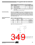
4. The Flash is programmed one page at a time. The memory page is loaded one
byte at a time by supplying the 7 LSB of the address and data together with the
Load Program Memory Page instruction. To ensure correct loading of the page,
the data low byte must be loaded before data high byte is applied for a given
address. The Program Memory Page is stored by loading the Write Program
Memory Page instruction with the address lines 15..8. Before issuing this com-
mand, make sure the instruction Load Extended Address Byte has been used to
define the MSB of the address. The extended address byte is stored until the
command is re-issued, i.e., the command needs only be issued for the first page,
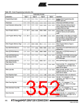
and when crossing the 64KWord boundary. If polling (RDY/BSY) is not used, the
user must wait at least tWD_FLASH before issuing the next page. (See Table 162.)
Accessing the serial programming interface before the Flash write operation
completes can result in incorrect programming.
5. The EEPROM array is programmed one byte at a time by supplying the address
and data together with the appropriate Write instruction. An EEPROM memory
location is first automatically erased before new data is written. If polling is not
used, the user must wait at least tWD_EEPROM before issuing the next byte. (See
Table 162.) In a chip erased device, no 0xFFs in the data file(s) need to be
programmed.
6. Any memory location can be verified by using the Read instruction which returns
the content at the selected address at serial output PDO. When reading the
350
ATmega640/1280/1281/2560/2561
2549A–AVR–03/05

 ATMEL [ ATMEL ]