ATmega640/1280/1281/2560/2561
1. 1. Set XA1, XA0 to “10”. This enables command loading.
2. Set DATA to “0000 0000”. This is the command for No Operation.
3. Give XTAL1 a positive pulse. This loads the command, and the internal write sig-
nals are reset.
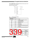
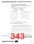
Figure 140. Addressing the Flash Which is Organized in Pages(1)
PCMSB
PAGEMSB
PROGRAM
COUNTER
PCPAGE
PCWORD
PAGE ADDRESS
WITHIN THE FLASH
WORD ADDRESS
WITHIN A PAGE
PROGRAM MEMORY
PAGE
PAGE
INSTRUCTION WORD
PCWORD[PAGEMSB:0]:
00
01
02
PAGEEND
Note:
1. PCPAGE and PCWORD are listed in Table 158 on page 340.
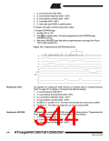
Figure 141. Programming the Flash Waveforms(1)
F
A
B
C
D
E
B
C
D
E
G
I
H
0x10
ADDR. LOW
DATA LOW
DATA HIGH
ADDR. LOW DATA LOW
DATA HIGH
ADDR. HIGH
ADDR. EXT.H
XX
XX
XX
DATA
XA1
XA0
BS1
BS2
XTAL1
WR
RDY/BSY
RESET +12V
OE
PAGEL
Note:
1. “XX” is don’t care. The letters refer to the programming description above.
Programming the EEPROM
The EEPROM is organized in pages, see Table 159 on page 340. When programming
the EEPROM, the program data is latched into a page buffer. This allows one page of
data to be programmed simultaneously. The programming algorithm for the EEPROM
data memory is as follows (refer to “Programming the Flash” on page 341 for details on
Command, Address and Data loading):
343
2549A–AVR–03/05

 ATMEL [ ATMEL ]