page address is taken from the high part of the Z-pointer. The data in R1 and R0 are
ignored. The PGWRT bit will auto-clear upon completion of a Page Write, or if no SPM
instruction is executed within four clock cycles. The CPU is halted during the entire
Page Write operation if the NRWW section is addressed.
• Bit 1 – PGERS: Page Erase
If this bit is written to one at the same time as SPMEN, the next SPM instruction within
four clock cycles executes Page Erase. The page address is taken from the high part of
the Z-pointer. The data in R1 and R0 are ignored. The PGERS bit will auto-clear upon
completion of a Page Erase, or if no SPM instruction is executed within four clock
cycles. The CPU is halted during the entire Page Write operation if the NRWW section is
addressed.
• Bit 0 – SPMEN: Store Program Memory Enable
This bit enables the SPM instruction for the next four clock cycles. If written to one
together with either RWWSRE, BLBSET, PGWRT’ or PGERS, the following SPM
instruction will have a special meaning, see description above. If only SPMEN is written,
the following SPM instruction will store the value in R1:R0 in the temporary page buffer
addressed by the Z-pointer. The LSB of the Z-pointer is ignored. The SPMEN bit will
auto-clear upon completion of an SPM instruction, or if no SPM instruction is executed
within four clock cycles. During Page Erase and Page Write, the SPMEN bit remains
high until the operation is completed.
Writing any other combination than “10001”, “01001”, “00101”, “00011” or “00001” in the
lower five bits will have no effect.
Note:
Only one SPM instruction should be active at any time.
Addressing the Flash
During Self-
Programming
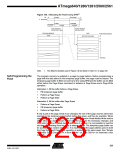
The Z-pointer is used to address the SPM commands. The Z pointer consists of the Z-
registers ZL and ZH in the register file, and RAMPZ in the I/O space. The number of bits
actually used is implementation dependent. Note that the RAMPZ register is only imple-
mented when the program space is larger than 64K bytes.
Bit
23
15
22
14
21
13
20
12
19
11
18
10
17
16
9
8
RAMPZ
ZH (R31)
ZL (R30)
RAMPZ7
Z15
Z7
RAMPZ6
Z14
Z6
RAMPZ5
Z13
Z5
RAMPZ4
Z12
Z4
RAMPZ3
Z11
Z3
RAMPZ2
Z10
Z2
RAMPZ1
RAMPZ0
Z9
Z1
1
Z8
Z0
0
7
6
5
4
3
2
Since the Flash is organized in pages (see Table 158 on page 340), the Program
Counter can be treated as having two different sections. One section, consisting of the
least significant bits, is addressing the words within a page, while the most significant
bits are addressing the pages. This is shown in Figure 138. Note that the Page Erase
and Page Write operations are addressed independently. Therefore it is of major impor-
tance that the Boot Loader software addresses the same page in both the Page Erase
and Page Write operation. Once a programming operation is initiated, the address is
latched and the Z-pointer can be used for other operations.
The (E)LPM instruction use the Z-pointer to store the address. Since this instruction
addresses the Flash byte-by-byte, also bit Z0 of the Z-pointer is used.
322
ATmega640/1280/1281/2560/2561
2549A–AVR–03/05

 ATMEL [ ATMEL ]