ATmega640/1280/1281/2560/2561
Store Program Memory
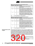
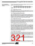
The Store Program Memory Control and Status Register contains the control bits
Control and Status Register – needed to control the Boot Loader operations.
SPMCSR
Bit
7
SPMIE
R/W
0
6
5
SIGRD
R/W
0
4
RWWSRE
R/W
3
BLBSET
R/W
0
2
PGWRT
R/W
0
1
PGERS
R/W
0
0
SPMEN
R/W
0
RWWSB
SPMCSR
Read/Write
Initial Value
R
0
0
• Bit 7 – SPMIE: SPM Interrupt Enable
When the SPMIE bit is written to one, and the I-bit in the Status Register is set (one), the
SPM ready interrupt will be enabled. The SPM ready Interrupt will be executed as long
as the SPMEN bit in the SPMCSR Register is cleared.
• Bit 6 – RWWSB: Read-While-Write Section Busy
When a Self-Programming (Page Erase or Page Write) operation to the RWW section is
initiated, the RWWSB will be set (one) by hardware. When the RWWSB bit is set, the
RWW section cannot be accessed. The RWWSB bit will be cleared if the RWWSRE bit
is written to one after a Self-Programming operation is completed. Alternatively the
RWWSB bit will automatically be cleared if a page load operation is initiated.
• Bit 5 – SIGRD: Signature Row Read
If this bit is written to one at the same time as SPMEN, the next LPM instruction within
three clock cycles will read a byte from the signature row into the destination register.
see “Reading the Signature Row from Software” on page 326 for details. An SPM
instruction within four cycles after SIGRD and SPMEN are set will have no effect. This
operation is reserved for future use and should not be used.
• Bit 4 – RWWSRE: Read-While-Write Section Read Enable
When programming (Page Erase or Page Write) to the RWW section, the RWW section
is blocked for reading (the RWWSB will be set by hardware). To re-enable the RWW
section, the user software must wait until the programming is completed (SPMEN will be
cleared). Then, if the RWWSRE bit is written to one at the same time as SPMEN, the
next SPM instruction within four clock cycles re-enables the RWW section. The RWW
section cannot be re-enabled while the Flash is busy with a Page Erase or a Page Write
(SPMEN is set). If the RWWSRE bit is written while the Flash is being loaded, the Flash
load operation will abort and the data loaded will be lost.
• Bit 3 – BLBSET: Boot Lock Bit Set
If this bit is written to one at the same time as SPMEN, the next SPM instruction within
four clock cycles sets Boot Lock bits, according to the data in R0. The data in R1 and
the address in the Z-pointer are ignored. The BLBSET bit will automatically be cleared
upon completion of the Lock bit set, or if no SPM instruction is executed within four clock
cycles.
An (E)LPM instruction within three cycles after BLBSET and SPMEN are set in the
SPMCSR Register, will read either the Lock bits or the Fuse bits (depending on Z0 in
the Z-pointer) into the destination register. See “Reading the Fuse and Lock Bits from
Software” on page 325 for details.
• Bit 2 – PGWRT: Page Write
If this bit is written to one at the same time as SPMEN, the next SPM instruction within
four clock cycles executes Page Write, with the data stored in the temporary buffer. The
321
2549A–AVR–03/05

 ATMEL [ ATMEL ]