ATmega640/1280/1281/2560/2561
•
•
•
•
•
•
After the TWI has transmitted SLA+R/W.
After the TWI has transmitted an address byte.
After the TWI has lost arbitration.
After the TWI has been addressed by own slave address or general call.
After the TWI has received a data byte.
After a STOP or REPEATED START has been received while still addressed as a
Slave.
•
When a bus error has occurred due to an illegal START or STOP condition.
TWI Register Description
TWI Bit Rate Register – TWBR
Bit
7
TWBR7
R/W
0
6
TWBR6
R/W
0
5
TWBR5
R/W
0
4
TWBR4
R/W
0
3
TWBR3
R/W
0
2
TWBR2
R/W
0
1
TWBR1
R/W
0
0
TWBR0
R/W
0
TWBR
Read/Write
Initial Value
• Bits 7..0 – TWI Bit Rate Register
TWBR selects the division factor for the bit rate generator. The bit rate generator is a
frequency divider which generates the SCL clock frequency in the Master modes. See
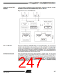
“Bit Rate Generator Unit” on page 247 for calculating bit rates.
TWI Control Register – TWCR
Bit
7
TWINT
R/W
0
6
TWEA
R/W
0
5
TWSTA
R/W
0
4
TWSTO
R/W
0
3
2
TWEN
R/W
0
1
–
0
TWIE
R/W
0
TWWC
TWCR
Read/Write
Initial Value
R
0
R
0
The TWCR is used to control the operation of the TWI. It is used to enable the TWI, to
initiate a Master access by applying a START condition to the bus, to generate a
Receiver acknowledge, to generate a stop condition, and to control halting of the bus
while the data to be written to the bus are written to the TWDR. It also indicates a write
collision if data is attempted written to TWDR while the register is inaccessible.
• Bit 7 – TWINT: TWI Interrupt Flag
This bit is set by hardware when the TWI has finished its current job and expects appli-
cation software response. If the I-bit in SREG and TWIE in TWCR are set, the MCU will
jump to the TWI Interrupt Vector. While the TWINT Flag is set, the SCL low period is
stretched. The TWINT Flag must be cleared by software by writing a logic one to it. Note
that this flag is not automatically cleared by hardware when executing the interrupt rou-
tine. Also note that clearing this flag starts the operation of the TWI, so all accesses to
the TWI Address Register (TWAR), TWI Status Register (TWSR), and TWI Data Regis-
ter (TWDR) must be complete before clearing this flag.
• Bit 6 – TWEA: TWI Enable Acknowledge Bit
The TWEA bit controls the generation of the acknowledge pulse. If the TWEA bit is writ-
ten to one, the ACK pulse is generated on the TWI bus if the following conditions are
met:
1. The device’s own slave address has been received.
2. A general call has been received, while the TWGCE bit in the TWAR is set.
249
2549A–AVR–03/05

 ATMEL [ ATMEL ]