ATmega640/1280/1281/2560/2561
Overview of the TWI
Module
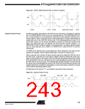
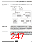
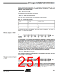
The TWI module is comprised of several submodules, as shown in Figure 99. All regis-
ters drawn in a thick line are accessible through the AVR data bus.
Figure 99. Overview of the TWI Module
SCL
SDA
Spike
Filter
Spike
Filter
Slew-rate
Control
Slew-rate
Control
Bus Interface Unit
Bit Rate Generator
START / STOP
Spike Suppression
Prescaler
Control
Address/Data Shift
Register (TWDR)
Bit Rate Register
(TWBR)
Arbitration detection
Ack
Address Match Unit
Control Unit
Address Register
(TWAR)
Status Register
(TWSR)
Control Register
(TWCR)
State Machine and
Status control
Address Comparator
SCL and SDA Pins
These pins interface the AVR TWI with the rest of the MCU system. The output drivers
contain a slew-rate limiter in order to conform to the TWI specification. The input stages
contain a spike suppression unit removing spikes shorter than 50 ns. Note that the inter-
nal pull-ups in the AVR pads can be enabled by setting the PORT bits corresponding to
the SCL and SDA pins, as explained in the I/O Port section. The internal pull-ups can in
some systems eliminate the need for external ones.
Bit Rate Generator Unit
This unit controls the period of SCL when operating in a Master mode. The SCL period
is controlled by settings in the TWI Bit Rate Register (TWBR) and the Prescaler bits in
the TWI Status Register (TWSR). Slave operation does not depend on Bit Rate or Pres-
caler settings, but the CPU clock frequency in the Slave must be at least 16 times higher
than the SCL frequency. Note that slaves may prolong the SCL low period, thereby
reducing the average TWI bus clock period. The SCL frequency is generated according
to the following equation:
247
2549A–AVR–03/05

 ATMEL [ ATMEL ]