ATmega640/1280/1281/2560/2561
• Bit 4 – MSTR: Master/Slave Select
This bit selects Master SPI mode when written to one, and Slave SPI mode when written
logic zero. If SS is configured as an input and is driven low while MSTR is set, MSTR will
be cleared, and SPIF in SPSR will become set. The user will then have to set MSTR to
re-enable SPI Master mode.
• Bit 3 – CPOL: Clock Polarity
When this bit is written to one, SCK is high when idle. When CPOL is written to zero,
SCK is low when idle. Refer to Figure 81 and Figure 82 for an example. The CPOL func-
tionality is summarized below:
Table 94. CPOL Functionality
CPOL
Leading Edge
Rising
Trailing Edge
Falling
0
1
Falling
Rising
• Bit 2 – CPHA: Clock Phase
The settings of the Clock Phase bit (CPHA) determine if data is sampled on the leading
(first) or trailing (last) edge of SCK. Refer to Figure 81 and Figure 82 for an example.
The CPOL functionality is summarized below:
Table 95. CPHA Functionality
CPHA
Leading Edge
Sample
Trailing Edge
Setup
0
1
Setup
Sample
• Bits 1, 0 – SPR1, SPR0: SPI Clock Rate Select 1 and 0
These two bits control the SCK rate of the device configured as a Master. SPR1 and
SPR0 have no effect on the Slave. The relationship between SCK and the Oscillator
Clock frequency fosc is shown in the following table:
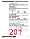
Table 96. Relationship Between SCK and the Oscillator Frequency
SPI2X
SPR1
SPR0
SCK Frequency
fosc/4
0
0
0
0
1
1
1
1
0
0
1
1
0
0
1
1
0
1
0
1
0
1
0
1
fosc/16
fosc/64
fosc/128
fosc/2
fosc/8
fosc/32
fosc/64
201
2549A–AVR–03/05

 ATMEL [ ATMEL ]