ATmega640/1280/1281/2560/2561
16-bit Timer/Counter The 16-bit Timer/Counter unit allows accurate program execution timing (event man-
agement), wave generation, and signal timing measurement. The main features are:
• True 16-bit Design (i.e., Allows 16-bit PWM)
• Three independent Output Compare Units
• Double Buffered Output Compare Registers
(Timer/Counter1,
Timer/Counter3,
Timer/Counter4 and
• One Input Capture Unit
• Input Capture Noise Canceler
Timer/Counter5)
• Clear Timer on Compare Match (Auto Reload)
• Glitch-free, Phase Correct Pulse Width Modulator (PWM)
• Variable PWM Period
• Frequency Generator
• External Event Counter
• Twenty independent interrupt sources (TOV1, OCF1A, OCF1B, OCF1C, ICF1, TOV3,
OCF3A, OCF3B, OCF3C, ICF3, TOV4, OCF4A, OCF4B, OCF4C, ICF4, TOV5, OCF5A,
OCF5B, OCF5C and ICF5)
Overview
Most register and bit references in this section are written in general form. A lower case
“n” replaces the Timer/Counter number, and a lower case “x” replaces the Output Com-
pare unit channel. However, when using the register or bit defines in a program, the
precise form must be used, i.e., TCNT1 for accessing Timer/Counter1 counter value
and so on.
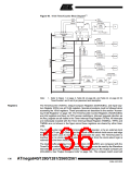
A simplified block diagram of the 16-bit Timer/Counter is shown in Figure 49. For the
actual placement of I/O pins, see “Pinout ATmega640/1280/2560” on page 2 and
“Pinout ATmega1281/2561” on page 3. CPU accessible I/O Registers, including I/O bits
and I/O pins, are shown in bold. The device-specific I/O Register and bit locations are
listed in the “16-bit Timer/Counter Register Description” on page 157.
The Power Reduction Timer/Counter1 bit, PRTIM1, in “Power Reduction Register 0 -
PRR0” on page 54 must be written to zero to enable Timer/Counter1 module.
The Power Reduction Timer/Counter3 bit, PRTIM3, in “Power Reduction Register 1 -
PRR1” on page 55 must be written to zero to enable Timer/Counter3 module.
The Power Reduction Timer/Counter4 bit, PRTIM4, in “Power Reduction Register 1 -
PRR1” on page 55 must be written to zero to enable Timer/Counter4 module.
The Power Reduction Timer/Counter5 bit, PRTIM5, in “Power Reduction Register 1 -
PRR1” on page 55 must be written to zero to enable Timer/Counter5 module.
Timer/Counter4 and Timer/Counter5 only have full functionality in the
ATmega640/1280/2560.
135
2549A–AVR–03/05

 ATMEL [ ATMEL ]