Match. To ensure symmetry around BOTTOM the OCn value at MAX must
correspond to the result of an up-counting Compare Match.
•
The timer starts counting from a value higher than the one in OCR0A, and for that
reason misses the Compare Match and hence the OCn change that would have
happened on the way up.
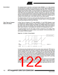
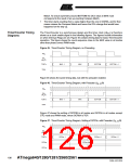
Timer/Counter Timing
Diagrams
The Timer/Counter is a synchronous design and the timer clock (clkT0) is therefore
shown as a clock enable signal in the following figures. The figures include information
on when Interrupt Flags are set. Figure 45 contains timing data for basic Timer/Counter
operation. The figure shows the count sequence close to the MAX value in all modes
other than phase correct PWM mode.
Figure 45. Timer/Counter Timing Diagram, no Prescaling
clkI/O
clkTn
(clkI/O/1)
TCNTn
TOVn
MAX - 1
MAX
BOTTOM
BOTTOM + 1
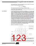
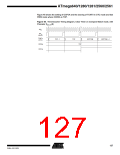
Figure 46 shows the same timing data, but with the prescaler enabled.
Figure 46. Timer/Counter Timing Diagram, with Prescaler (fclk_I/O/8)
clkI/O
clkTn
(clkI/O/8)
TCNTn
TOVn
MAX - 1
MAX
BOTTOM
BOTTOM + 1
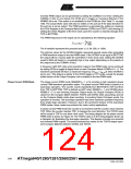
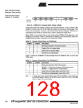
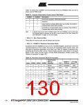
Figure 47 shows the setting of OCF0B in all modes and OCF0A in all modes except
CTC mode and PWM mode, where OCR0A is TOP.
Figure 47. Timer/Counter Timing Diagram, Setting of OCF0x, with Prescaler (fclk_I/O/8)
clkI/O
clkTn
(clkI/O/8)
TCNTn
OCRnx
OCFnx
OCRnx - 1
OCRnx
OCRnx + 1
OCRnx + 2
OCRnx Value
126
ATmega640/1280/1281/2560/2561
2549A–AVR–03/05

 ATMEL [ ATMEL ]