ATmega640/1280/1281/2560/2561
mum frequency of fOC0 = fclk_I/O/2 when OCR0A is set to zero (0x00). The waveform
frequency is defined by the following equation:
f
clk_I/O
f
= -------------------------------------------------
OCnx
2 ⋅ N ⋅ (1 + OCRnx)
The N variable represents the prescale factor (1, 8, 64, 256, or 1024).
As for the Normal mode of operation, the TOV0 Flag is set in the same timer clock cycle
that the counter counts from MAX to 0x00.
Fast PWM Mode
The fast Pulse Width Modulation or fast PWM mode (WGM02:0 = 3 or 7) provides a high
frequency PWM waveform generation option. The fast PWM differs from the other PWM
option by its single-slope operation. The counter counts from BOTTOM to TOP then
restarts from BOTTOM. TOP is defined as 0xFF when WGM2:0 = 3, and OCR0A when
WGM2:0 = 7. In non-inverting Compare Output mode, the Output Compare (OC0x) is
cleared on the Compare Match between TCNT0 and OCR0x, and set at BOTTOM. In
inverting Compare Output mode, the output is set on Compare Match and cleared at
BOTTOM. Due to the single-slope operation, the operating frequency of the fast PWM
mode can be twice as high as the phase correct PWM mode that use dual-slope opera-
tion. This high frequency makes the fast PWM mode well suited for power regulation,
rectification, and DAC applications. High frequency allows physically small sized exter-
nal components (coils, capacitors), and therefore reduces total system cost.
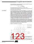
In fast PWM mode, the counter is incremented until the counter value matches the TOP
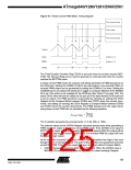
value. The counter is then cleared at the following timer clock cycle. The timing diagram
for the fast PWM mode is shown in Figure 43. The TCNT0 value is in the timing diagram
shown as a histogram for illustrating the single-slope operation. The diagram includes
non-inverted and inverted PWM outputs. The small horizontal line marks on the TCNT0
slopes represent Compare Matches between OCR0x and TCNT0.
Figure 43. Fast PWM Mode, Timing Diagram
OCRnx Interrupt Flag Set
OCRnx Update and
TOVn Interrupt Flag Set
TCNTn
(COMnx1:0 = 2)
(COMnx1:0 = 3)
OCnx
OCnx
1
2
3
4
5
6
7
Period
The Timer/Counter Overflow Flag (TOV0) is set each time the counter reaches TOP. If
the interrupt is enabled, the interrupt handler routine can be used for updating the com-
pare value.
In fast PWM mode, the compare unit allows generation of PWM waveforms on the
OC0x pins. Setting the COM0x1:0 bits to two will produce a non-inverted PWM and an
123
2549A–AVR–03/05

 ATMEL [ ATMEL ]