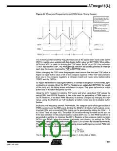
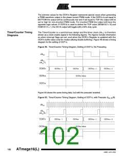
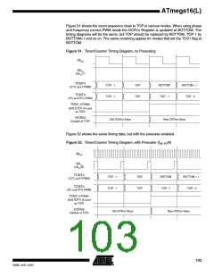
ATmega16(L)
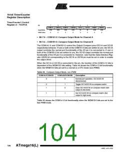
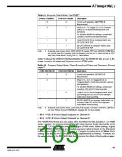
Table 45. Compare Output Mode, Fast PWM(1)
COM1A1/COM1B1
COM1A0/COM1B0
Description
0
0
Normal port operation, OC1A/OC1B
disconnected.
0
1
WGM13:0 = 15: Toggle OC1A on Compare
Match, OC1B disconnected (normal port
operation).
For all other WGM13:0 settings, normal port
operation, OCnA/OCnB disconnected.
1
1
0
1
Clear OC1A/OC1B on compare match, set
OC1A/OC1B at TOP
Set OC1A/OC1B on compare match, clear
OC1A/OC1B at TOP
Note:
1. A special case occurs when OCR1A/OCR1B equals TOP and COM1A1/COM1B1 is
set. In this case the compare match is ignored, but the set or clear is done at TOP.
See “Fast PWM Mode” on page 96. for more details.
Table 46 shows the COM1x1:0 bit functionality when the WGM13:0 bits are set to the
phase correct or the phase and frequency correct, PWM mode.
Table 46. Compare Output Mode, Phase Correct and Phase and Frequency Correct
PWM (1)
COM1A1/COM1B1
COM1A0/COM1B0
Description
0
0
Normal port operation, OC1A/OC1B
disconnected.
0
1
WGM13:0 = 9 or 14: Toggle OCnA on
Compare Match, OCnB disconnected (normal
port operation).
For all other WGM13:0 settings, normal port
operation, OC1A/OC1B disconnected.
1
1
0
1
Clear OC1A/OC1B on compare match when
up-counting. Set OC1A/OC1B on compare
match when downcounting.
Set OC1A/OC1B on compare match when up-
counting. Clear OC1A/OC1B on compare
match when downcounting.
Note:
1. A special case occurs when OCR1A/OCR1B equals TOP and COM1A1/COM1B1 is
set. See “Phase Correct PWM Mode” on page 98. for more details.
• Bit 3 – FOC1A: Force Output Compare for Channel A
• Bit 2 – FOC1B: Force Output Compare for Channel B
The FOC1A/FOC1B bits are only active when the WGM13:0 bits specifies a non-PWM
mode. However, for ensuring compatibility with future devices, these bits must be set to
zero when TCCR1A is written when operating in a PWM mode. When writing a logical
one to the FOC1A/FOC1B bit, an immediate compare match is forced on the Waveform
Generation unit. The OC1A/OC1B output is changed according to its COM1x1:0 bits
setting. Note that the FOC1A/FOC1B bits are implemented as strobes. Therefore it is
the value present in the COM1x1:0 bits that determine the effect of the forced compare.
105
2466E–AVR–10/02

 ATMEL [ ATMEL ]