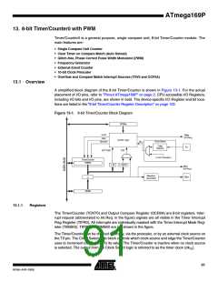
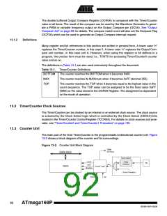
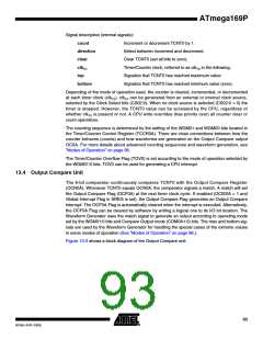
ATmega169P
13.4.3
Using the Output Compare Unit
Since writing TCNT0 in any mode of operation will block all compare matches for one timer clock
cycle, there are risks involved when changing TCNT0 when using the Output Compare unit,
independently of whether the Timer/Counter is running or not. If the value written to TCNT0
equals the OCR0A value, the compare match will be missed, resulting in incorrect waveform
generation. Similarly, do not write the TCNT0 value equal to BOTTOM when the counter is
downcounting.
The setup of the OC0A should be performed before setting the Data Direction Register for the
port pin to output. The easiest way of setting the OC0A value is to use the Force Output Com-
pare (FOC0A) strobe bits in Normal mode. The OC0A Register keeps its value even when
changing between Waveform Generation modes.
Be aware that the COM0A1:0 bits are not double buffered together with the compare value.
Changing the COM0A1:0 bits will take effect immediately.
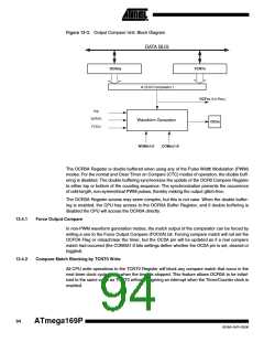
13.5 Compare Match Output Unit
The Compare Output mode (COM0A1:0) bits have two functions. The Waveform Generator
uses the COM0A1:0 bits for defining the Output Compare (OC0A) state at the next compare
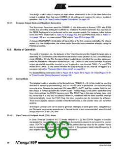
match. Also, the COM0A1:0 bits control the OC0A pin output source. Figure 13-4 shows a sim-
plified schematic of the logic affected by the COM0A1:0 bit setting. The I/O Registers, I/O bits,
and I/O pins in the figure are shown in bold. Only the parts of the general I/O port control regis-
ters (DDR and PORT) that are affected by the COM0A1:0 bits are shown. When referring to the
OC0A state, the reference is for the internal OC0A Register, not the OC0A pin. If a System
Reset occur, the OC0A Register is reset to “0”.
Figure 13-4. Compare Match Output Unit, Schematic
COMnx1
Waveform
Generator
COMnx0
FOCn
D
Q
1
0
OCn
Pin
OCnx
D
Q
PORT
D
Q
DDR
clkI/O
The general I/O port function is overridden by the Output Compare (OC0A) from the Waveform
Generator if either of the COM0A1:0 bits are set. However, the OC0A pin direction (input or out-
put) is still controlled by the Data Direction Register (DDR) for the port pin. The Data Direction
Register bit for the OC0A pin (DDR_OC0A) must be set as output before the OC0A value is vis-
ible on the pin. The port override function is independent of the Waveform Generation mode.
95
8018A–AVR–03/06

 ATMEL [ ATMEL ]