6.4
EEPROM Register Description
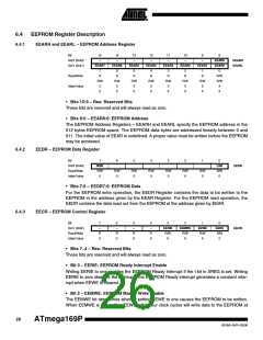
6.4.1
EEARH and EEARL – EEPROM Address Register
Bit
15
14
13
12
11
10
9
8
EEAR8
EEAR0
0
0x22 (0x42)
0x21 (0x41)
–
–
–
–
–
–
–
EEARH
EEARL
EEAR7
EEAR6
EEAR5
EEAR4
EEAR3
EEAR2
EEAR1
7
R
6
R
5
R
4
R
3
R
2
R
1
R
Read/Write
Initial Value
R/W
R/W
X
R/W
0
R/W
0
R/W
0
R/W
0
R/W
0
R/W
0
R/W
0
X
X
X
X
X
X
X
X
• Bits 15:9 – Res: Reserved Bits
These bits are reserved and will always read as zero.
• Bits 8:0 – EEAR8:0: EEPROM Address
The EEPROM Address Registers – EEARH and EEARL specify the EEPROM address in the
512 bytes EEPROM space. The EEPROM data bytes are addressed linearly between 0 and
511. The initial value of EEAR is undefined. A proper value must be written before the EEPROM
may be accessed.
6.4.2
EEDR – EEPROM Data Register
Bit
7
6
5
4
3
2
1
0
0x20 (0x40)
Read/Write
Initial Value
MSB
R/W
0
LSB
R/W
0
EEDR
R/W
0
R/W
0
R/W
0
R/W
0
R/W
0
R/W
0
• Bits 7:0 – EEDR7:0: EEPROM Data
For the EEPROM write operation, the EEDR Register contains the data to be written to the
EEPROM in the address given by the EEAR Register. For the EEPROM read operation, the
EEDR contains the data read out from the EEPROM at the address given by EEAR.
6.4.3
EECR – EEPROM Control Register
Bit
0x1F (0x3F)
7
6
–
5
–
4
–
3
EERIE
R/W
0
2
EEMWE
R/W
0
1
EEWE
R/W
X
0
EERE
R/W
0
–
EECR
Read/Write
Initial Value
R
0
R
0
R
0
R
0
• Bits 7..4 – Res: Reserved Bits
These bits are reserved and will always read as zero.
• Bit 3 – EERIE: EEPROM Ready Interrupt Enable
Writing EERIE to one enables the EEPROM Ready Interrupt if the I bit in SREG is set. Writing
EERIE to zero disables the interrupt. The EEPROM Ready interrupt generates a constant inter-
rupt when EEWE is cleared.
• Bit 2 – EEMWE: EEPROM Master Write Enable
The EEMWE bit determines whether setting EEWE to one causes the EEPROM to be written.
When EEMWE is set, setting EEWE within four clock cycles will write data to the EEPROM at
26
ATmega169P
8018A–AVR–03/06

 ATMEL [ ATMEL ]