23.7 On-chip Debug Related Register in I/O Memory
23.7.1
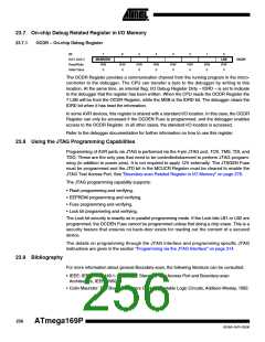
OCDR – On-chip Debug Register
Bit
7
6
5
4
3
2
1
0
0x31 (0x51)
Read/Write
Initial Value
MSB/IDRD
LSB
R/W
0
OCDR
R/W
0
R/W
0
R/W
0
R/W
0
R/W
0
R/W
0
R/W
0
The OCDR Register provides a communication channel from the running program in the micro-
controller to the debugger. The CPU can transfer a byte to the debugger by writing to this
location. At the same time, an internal flag; I/O Debug Register Dirty – IDRD – is set to indicate
to the debugger that the register has been written. When the CPU reads the OCDR Register the
7 LSB will be from the OCDR Register, while the MSB is the IDRD bit. The debugger clears the
IDRD bit when it has read the information.
In some AVR devices, this register is shared with a standard I/O location. In this case, the OCDR
Register can only be accessed if the OCDEN Fuse is programmed, and the debugger enables
access to the OCDR Register. In all other cases, the standard I/O location is accessed.
Refer to the debugger documentation for further information on how to use this register.
23.8 Using the JTAG Programming Capabilities
Programming of AVR parts via JTAG is performed via the 4-pin JTAG port, TCK, TMS, TDI, and
TDO. These are the only pins that need to be controlled/observed to perform JTAG program-
ming (in addition to power pins). It is not required to apply 12V externally. The JTAGEN Fuse
must be programmed and the JTD bit in the MCUCR Register must be cleared to enable the
JTAG Test Access Port. See ”Boundary-scan Related Register in I/O Memory” on page 278.
The JTAG programming capability supports:
• Flash programming and verifying.
• EEPROM programming and verifying.
• Fuse programming and verifying.
• Lock bit programming and verifying.
The Lock bit security is exactly as in parallel programming mode. If the Lock bits LB1 or LB2 are
programmed, the OCDEN Fuse cannot be programmed unless first doing a chip erase. This is a
security feature that ensures no back-door exists for reading out the content of a secured
device.
The details on programming through the JTAG interface and programming specific JTAG
instructions are given in the section ”Programming via the JTAG Interface” on page 314.
23.9 Bibliography
For more information about general Boundary-scan, the following literature can be consulted:
• IEEE: IEEE Std. 1149.1-1990. IEEE Standard Test Access Port and Boundary-scan
Architecture, IEEE, 1993.
• Colin Maunder: The Board Designers Guide to Testable Logic Circuits, Addison-Wesley, 1992.
256
ATmega169P
8018A–AVR–03/06

 ATMEL [ ATMEL ]