24.3 Data Registers
The Data Registers relevant for Boundary-scan operations are:
• Bypass Register
• Device Identification Register
• Reset Register
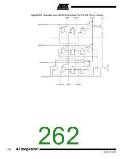
• Boundary-scan Chain
24.3.1
24.3.2
Bypass Register
The Bypass Register consists of a single Shift Register stage. When the Bypass Register is
selected as path between TDI and TDO, the register is reset to 0 when leaving the Capture-DR
controller state. The Bypass Register can be used to shorten the scan chain on a system when
the other devices are to be tested.
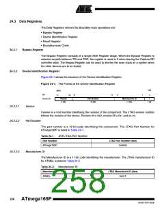
Device Identification Register
Figure 24-1 shows the structure of the Device Identification Register.
Figure 24-1. The Format of the Device Identification Register
LSB
MSB
Bit
31
28
27
12
11
1
0
Device ID
Version
Part Number
Manufacturer ID
1
4 bits
16 bits
11 bits
1-bit
24.3.2.1
24.3.2.2
Version
Version is a 4-bit number identifying the revision of the component. The JTAG version number
follows the revision of the device. Revision A is 0x0, revision B is 0x1 and so on.
Part Number
The part number is a 16-bit code identifying the component. The JTAG Part Number for
ATmega169P is listed in Table 24-1.
Table 24-1. AVR JTAG Part Number
Part Number
JTAG Part Number (Hex)
ATmega169P
0x9405
24.3.2.3
Manufacturer ID
The Manufacturer ID is a 11-bit code identifying the manufacturer. The JTAG manufacturer ID
for ATMEL is listed in Table 24-2.
Table 24-2. Manufacturer ID
Manufacturer
JTAG Manufactor ID (Hex)
ATMEL
0x01F
258
ATmega169P
8018A–AVR–03/06

 ATMEL [ ATMEL ]