ATmega169P
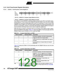
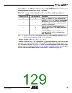
Table 14-3 shows the COM1x1:0 bit functionality when the WGM13:0 bits are set to the phase
correct or the phase and frequency correct, PWM mode.
Table 14-3. Compare Output Mode, Phase Correct and Phase and Frequency Correct
PWM(1)
COM1A1/COM1B1
COM1A0/COM1B0
Description
0
0
Normal port operation, OC1A/OC1B disconnected.
WGM13:0 = 8, 9, 10 or 11: Toggle OC1A on Compare
Match, OC1B disconnected (normal port operation).
For all other WGM1 settings, normal port operation,
OC1A/OC1B disconnected.
0
1
Clear OC1A/OC1B on Compare Match when up-
counting. Set OC1A/OC1B on Compare Match when
downcounting.
1
1
0
1
Set OC1A/OC1B on Compare Match when up-
counting. Clear OC1A/OC1B on Compare Match
when downcounting.
Note:
1. A special case occurs when OCR1A/OCR1B equals TOP and COM1A1/COM1B1 is set. See
”Phase Correct PWM Mode” on page 122. for more details.
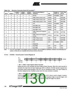
• Bit 1:0 – WGM11:0: Waveform Generation Mode
Combined with the WGM13:2 bits found in the TCCR1B Register, these bits control the counting
sequence of the counter, the source for maximum (TOP) counter value, and what type of wave-
form generation to be used, see Table 14-4. Modes of operation supported by the Timer/Counter
unit are: Normal mode (counter), Clear Timer on Compare match (CTC) mode, and three types
of Pulse Width Modulation (PWM) modes. (See ”Modes of Operation” on page 118.).
129
8018A–AVR–03/06

 ATMEL [ ATMEL ]