ATmega640/1280/1281/2560/2561
25. AC – Analog Comparator
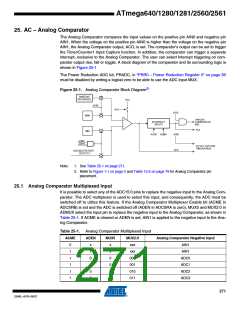
The Analog Comparator compares the input values on the positive pin AIN0 and negative pin
AIN1. When the voltage on the positive pin AIN0 is higher than the voltage on the negative pin
AIN1, the Analog Comparator output, ACO, is set. The comparator’s output can be set to trigger
the Timer/Counter1 Input Capture function. In addition, the comparator can trigger a separate
interrupt, exclusive to the Analog Comparator. The user can select Interrupt triggering on com-
parator output rise, fall or toggle. A block diagram of the comparator and its surrounding logic is
shown in Figure 25-1.
The Power Reduction ADC bit, PRADC, in “PRR0 – Power Reduction Register 0” on page 56
must be disabled by writing a logical zero to be able to use the ADC input MUX.
Figure 25-1. Analog Comparator Block Diagram(2)
BANDGAP
REFERENCE
ACBG
ACME
ADEN
ADC MULTIPLEXER
OUTPUT(1)
Note:
1. See Table 25-1 on page 271.
2. Refer to Figure 1-1 on page 2 and Table 13-5 on page 79 for Analog Comparator pin
placement.
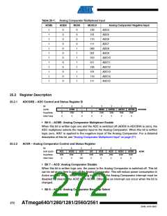
25.1 Analog Comparator Multiplexed Input
It is possible to select any of the ADC15:0 pins to replace the negative input to the Analog Com-
parator. The ADC multiplexer is used to select this input, and consequently, the ADC must be
switched off to utilize this feature. If the Analog Comparator Multiplexer Enable bit (ACME in
ADCSRB) is set and the ADC is switched off (ADEN in ADCSRA is zero), MUX5 and MUX2:0 in
ADMUX select the input pin to replace the negative input to the Analog Comparator, as shown in
Table 25-1. If ACME is cleared or ADEN is set, AIN1 is applied to the negative input to the Ana-
log Comparator.
Table 25-1. Analog Comparator Mulitiplexed Input
ACME
ADEN
MUX5
MUX2:0
xxx
Analog Comparator Negative Input
0
1
1
1
1
1
x
1
0
0
0
0
x
x
0
0
0
0
AIN1
AIN1
xxx
000
ADC0
ADC1
ADC2
ADC3
001
010
011
271
2549L–AVR–08/07

 ATMEL [ ATMEL ]