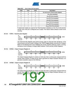
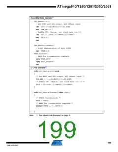
21. SPI – Serial Peripheral Interface
The Serial Peripheral Interface (SPI) allows high-speed synchronous data transfer between the
ATmega640/1280/1281/2560/2561 and peripheral devices or between several AVR devices.
The ATmega640/1280/1281/2560/2561 SPI includes the following features:
• Full-duplex, Three-wire Synchronous Data Transfer
• Master or Slave Operation
• LSB First or MSB First Data Transfer
• Seven Programmable Bit Rates
• End of Transmission Interrupt Flag
• Write Collision Flag Protection
• Wake-up from Idle Mode
• Double Speed (CK/2) Master SPI Mode
USART can also be used in Master SPI mode, see “USART in SPI Mode” on page 232.
The Power Reduction SPI bit, PRSPI, in “PRR0 – Power Reduction Register 0” on page 56 on
page 50 must be written to zero to enable SPI module.
Figure 21-1. SPI Block Diagram(1)
DIVIDER
/2/4/8/16/32/64/128
Note:
1. Refer to Figure 1-1 on page 2, and Table 13-6 on page 79 for SPI pin placement.
The interconnection between Master and Slave CPUs with SPI is shown in Figure 21-2. The sys-
tem consists of two shift Registers, and a Master clock generator. The SPI Master initiates the
communication cycle when pulling low the Slave Select SS pin of the desired Slave. Master and
196
ATmega640/1280/1281/2560/2561
2549L–AVR–08/07

 ATMEL [ ATMEL ]