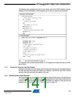
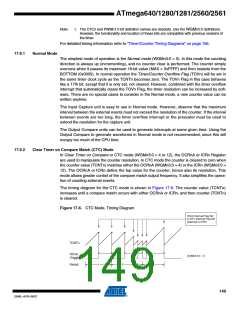
ATmega640/1280/1281/2560/2561
Measurement of an external signal’s duty cycle requires that the trigger edge is changed after
each capture. Changing the edge sensing must be done as early as possible after the ICRn
Register has been read. After a change of the edge, the Input Capture Flag (ICFn) must be
cleared by software (writing a logical one to the I/O bit location). For measuring frequency only,
the clearing of the ICFn Flag is not required (if an interrupt handler is used).
17.7 Output Compare Units
The 16-bit comparator continuously compares TCNTn with the Output Compare Register
(OCRnx). If TCNT equals OCRnx the comparator signals a match. A match will set the Output
Compare Flag (OCFnx) at the next timer clock cycle. If enabled (OCIEnx = 1), the Output Com-
pare Flag generates an Output Compare interrupt. The OCFnx Flag is automatically cleared
when the interrupt is executed. Alternatively the OCFnx Flag can be cleared by software by writ-
ing a logical one to its I/O bit location. The Waveform Generator uses the match signal to
generate an output according to operating mode set by the Waveform Generation mode
(WGMn3:0) bits and Compare Output mode (COMnx1:0) bits. The TOP and BOTTOM signals
are used by the Waveform Generator for handling the special cases of the extreme values in
some modes of operation (See “Modes of Operation” on page 148.)
A special feature of Output Compare unit A allows it to define the Timer/Counter TOP value (i.e.,
counter resolution). In addition to the counter resolution, the TOP value defines the period time
for waveforms generated by the Waveform Generator.
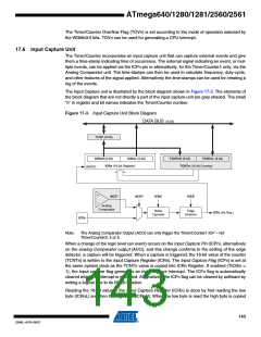
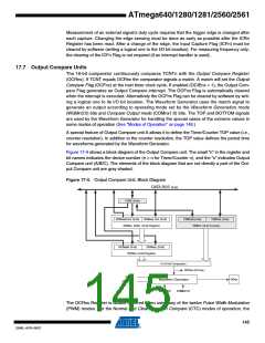
Figure 17-4 shows a block diagram of the Output Compare unit. The small “n” in the register and
bit names indicates the device number (n = n for Timer/Counter n), and the “x” indicates Output
Compare unit (A/B/C). The elements of the block diagram that are not directly a part of the Out-
put Compare unit are gray shaded.
Figure 17-4. Output Compare Unit, Block Diagram
DATA BUS (8-bit)
TEMP (8-bit)
OCRnxH Buf. (8-bit)
OCRnxL Buf. (8-bit)
TCNTnH (8-bit)
TCNTnL (8-bit)
OCRnx Buffer (16-bit Register)
TCNTn (16-bit Counter)
OCRnxH (8-bit)
OCRnxL (8-bit)
OCRnx (16-bit Register)
=
(16-bit Comparator )
OCFnx (Int.Req.)
TOP
OCnx
Waveform Generator
BOTTOM
WGMn3:0
COMnx1:0
The OCRnx Register is double buffered when using any of the twelve Pulse Width Modulation
(PWM) modes. For the Normal and Clear Timer on Compare (CTC) modes of operation, the
145
2549L–AVR–08/07

 ATMEL [ ATMEL ]