17.8.1
Compare Output Mode and Waveform Generation
The Waveform Generator uses the COMnx1:0 bits differently in normal, CTC, and PWM modes.
For all modes, setting the COMnx1:0 = 0 tells the Waveform Generator that no action on the
OCnx Register is to be performed on the next compare match. For compare output actions in the
non-PWM modes refer to Table 17-3 on page 160. For fast PWM mode refer to Table 17-4 on
page 160, and for phase correct and phase and frequency correct PWM refer to Table 17-5 on
page 160.
A change of the COMnx1:0 bits state will have effect at the first compare match after the bits are
written. For non-PWM modes, the action can be forced to have immediate effect by using the
FOCnx strobe bits.
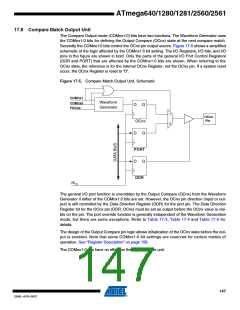
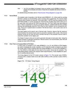
17.9 Modes of Operation
The mode of operation, i.e., the behavior of the Timer/Counter and the Output Compare pins, is
defined by the combination of the Waveform Generation mode (WGMn3:0) and Compare Output
mode (COMnx1:0) bits. The Compare Output mode bits do not affect the counting sequence,
while the Waveform Generation mode bits do. The COMnx1:0 bits control whether the PWM out-
put generated should be inverted or not (inverted or non-inverted PWM). For non-PWM modes
the COMnx1:0 bits control whether the output should be set, cleared or toggle at a compare
match (See “Compare Match Output Unit” on page 147.)
Table 17-2. Waveform Generation Mode Bit Description(1)
WGMn2
(CTCn)
WGMn1
(PWMn1) (PWMn0)
WGMn0
Timer/Counter
Mode of Operation
Update of
OCRnx at
TOVn Flag
Set on
Mode
WGMn3
TOP
0
1
2
3
4
5
6
7
0
0
0
0
0
0
0
0
0
0
0
0
1
1
1
1
0
0
1
1
0
0
1
1
0
1
0
1
0
1
0
1
Normal
PWM, Phase Correct, 8-bit
PWM, Phase Correct, 9-bit
PWM, Phase Correct, 10-bit
CTC
0xFFFF
0x00FF
0x01FF
0x03FF
OCRnA
0x00FF
0x01FF
0x03FF
Immediate
TOP
MAX
BOTTOM
BOTTOM
BOTTOM
MAX
TOP
TOP
Immediate
BOTTOM
BOTTOM
BOTTOM
Fast PWM, 8-bit
TOP
Fast PWM, 9-bit
TOP
Fast PWM, 10-bit
TOP
PWM, Phase and Frequency
8
9
1
1
0
0
0
0
0
1
ICRn
BOTTOM
BOTTOM
BOTTOM
BOTTOM
Correct
PWM,Phase and Frequency
OCRnA
Correct
10
11
12
13
14
15
1
1
1
1
1
1
0
0
1
1
1
1
1
1
0
0
1
1
0
1
0
1
0
1
PWM, Phase Correct
PWM, Phase Correct
CTC
ICRn
OCRnA
ICRn
–
TOP
TOP
BOTTOM
BOTTOM
MAX
Immediate
–
(Reserved)
–
Fast PWM
ICRn
OCRnA
BOTTOM
BOTTOM
TOP
Fast PWM
TOP
148
ATmega640/1280/1281/2560/2561
2549L–AVR–08/07

 ATMEL [ ATMEL ]