generation. Similarly, do not write the TCNT0 value equal to BOTTOM when the counter is
down-counting.
The setup of the OC0x should be performed before setting the Data Direction Register for the
port pin to output. The easiest way of setting the OC0x value is to use the Force Output Com-
pare (FOC0x) strobe bits in Normal mode. The OC0x Registers keep their values even when
changing between Waveform Generation modes.
Be aware that the COM0x1:0 bits are not double buffered together with the compare value.
Changing the COM0x1:0 bits will take effect immediately.
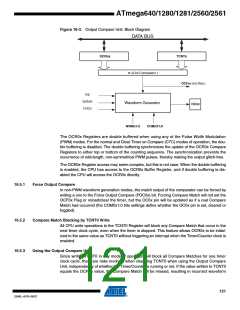
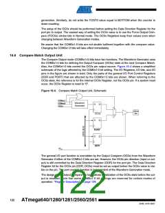
16.6 Compare Match Output Unit
The Compare Output mode (COM0x1:0) bits have two functions. The Waveform Generator uses
the COM0x1:0 bits for defining the Output Compare (OC0x) state at the next Compare Match.
Also, the COM0x1:0 bits control the OC0x pin output source. Figure 16-4 shows a simplified
schematic of the logic affected by the COM0x1:0 bit setting. The I/O Registers, I/O bits, and I/O
pins in the figure are shown in bold. Only the parts of the general I/O Port Control Registers
(DDR and PORT) that are affected by the COM0x1:0 bits are shown. When referring to the
OC0x state, the reference is for the internal OC0x Register, not the OC0x pin. If a system reset
occur, the OC0x Register is reset to “0”.
Figure 16-4. Compare Match Output Unit, Schematic
COMnx1
Waveform
Generator
COMnx0
FOCn
D
Q
1
0
OCnx
Pin
OCnx
D
Q
PORT
D
Q
DDR
clkI/O
The general I/O port function is overridden by the Output Compare (OC0x) from the Waveform
Generator if either of the COM0x1:0 bits are set. However, the OC0x pin direction (input or out-
put) is still controlled by the Data Direction Register (DDR) for the port pin. The Data Direction
Register bit for the OC0x pin (DDR_OC0x) must be set as output before the OC0x value is visi-
ble on the pin. The port override function is independent of the Waveform Generation mode.
The design of the Output Compare pin logic allows initialization of the OC0x state before the out-
put is enabled. Note that some COM0x1:0 bit settings are reserved for certain modes of
operation. “Register Description” on page 129.
122
ATmega640/1280/1281/2560/2561
2549L–AVR–08/07

 ATMEL [ ATMEL ]