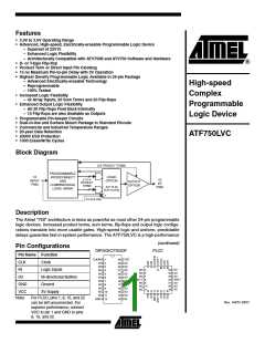
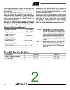
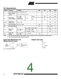
ATF750LVC
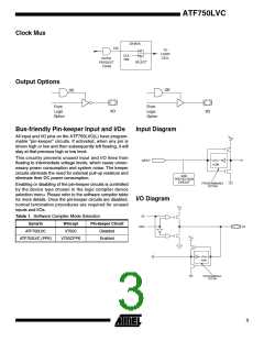
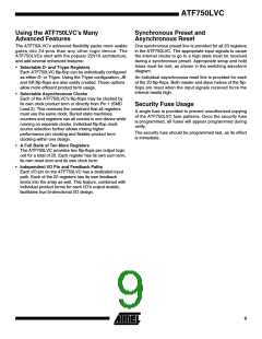
Clock Mux
CKMUX
CKi
TO
LOGIC
CELL
CLK
PIN
CLOCK
PRODUCT
TERM
SELECT
Output Options
Bus-friendly Pin-keeper Input and I/Os
Input Diagram
All input and I/O pins on the ATF750LVC(L) have program-
mable “pin-keeper” circuits. If activated, when any pin is
driven high or low and then subsequently left floating, it will
stay at that previous high or low level.
VCC
This circuitry prevents unused input and I/O lines from
floating to intermediate voltage levels, which cause unnec-
essary power consumption and system noise. The keeper
circuits eliminate the need for external pull-up resistors and
eliminate their DC power consumption.
INPUT
100K
ESD
PROTECTION
CIRCUIT
PROGRAMMABLE
OPTION
Enabling or disabling of the pin-keeper circuits is controlled
by the device type chosen in the logic compiler device
selection menu. Please refer to the software compiler table
for more details. Once the pin-keeper circuits are disabled,
normal termination procedures are required for unused
inputs and I/Os.
I/O Diagram
VCC
OE
Table 1. Software Compiler Mode Selection
Synario
ATF750LVC
Wincupl
V750C
Pin-keeper Circuit
Disabled
DATA
I/O
VCC
ATF750LVC (PPK)
V750CPPK
Enabled
100K
PROGRAMMABLE
OPTION
3
图片预览")
 ATMEL [ ATMEL ]