ATF750LVC
Using the ATF750LVC’s Many
Advanced Features
The ATF750LVC’s advanced flexibility packs more usable
gates into 24-pins than any other logic device. The
ATF750LVCs start with the popular 22V10 architecture,
and add several enhanced features:
Synchronous Preset and
Asynchronous Reset
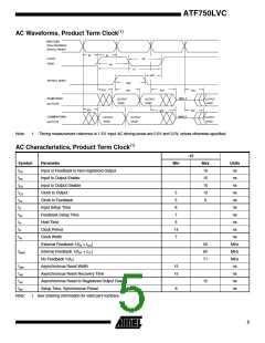
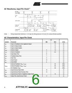
One synchronous preset line is provided for all 20 registers
in the ATF750LVC. The appropriate input signals to cause
the internal clocks to go to a high state must be received
during a synchronous preset. Appropriate setup and hold
times must be met, as shown in the switching waveform
diagram.
• Selectable D- and T-type Registers
Each ATF750LVC flip-flop can be individually configured
as either D- or T-type. Using the T-type configuration, JK
and SR flip-flops are also easily created. These options
allow more efficient product term usage.
An individual asynchronous reset line is provided for each
of the 20 flip-flops. Both master and slave halves of the flip-
flops are reset when the input signals received force the
internal resets high.
• Selectable Asynchronous Clocks
Each of the ATF750LVC’s flip-flops may be clocked by
its own clock product term or directly from Pin 1 (SMD
Lead 2). This removes the constraint that all registers
must use the same clock. Buried state machines,
counters and registers can all coexist in one device while
running on separate clocks. Individual flip-flop clock
source selection further allows mixing higher
performance pin clocking and flexible product term
clocking within one design.
Security Fuse Usage
A single fuse is provided to prevent unauthorized copying
of the ATF750LVC fuse patterns. Once the security fuse
is programmed, all fuses will appear programmed during
verify.
The security fuse should be programmed last, as its effect
is immediate.
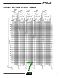
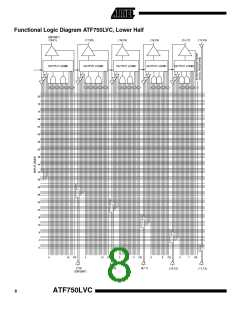
• A Full Bank of Ten More Registers
The ATF750LVC provides two flip-flops per output logic
cell for a total of 20. Each register has its own sum term,
its own reset term and its own clock term.
• Independent I/O Pin and Feedback Paths
Each I/O pin on the ATF750LVC has a dedicated input
path. Each of the 20 registers has its own feedback
terms into the array as well. This feature, combined with
individual product terms for each I/O’s output enable,
facilitates true bi-directional I/O design.
9
图片预览")
 ATMEL [ ATMEL ]