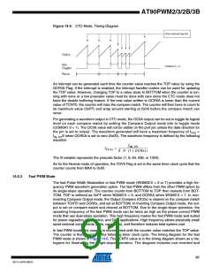
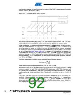
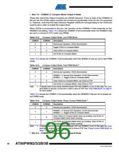
inverted PWM outputs. The small horizontal line marks on the TCNT0 slopes represent compare
matches between OCR0x and TCNT0.
Figure 14-6. Fast PWM Mode, Timing Diagram
OCRnx Interrupt Flag Set
OCRnx Update and
TOVn Interrupt Flag Set
TCNTn
(COMnx1:0 = 2)
(COMnx1:0 = 3)
OCn
OCn
1
2
3
4
5
6
7
Period
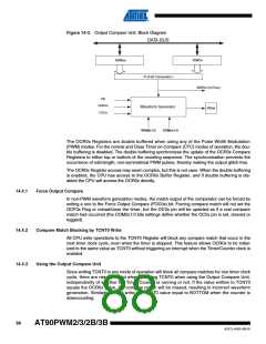
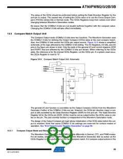
The Timer/Counter Overflow Flag (TOV0) is set each time the counter reaches TOP. If the inter-
rupt is enabled, the interrupt handler routine can be used for updating the compare value.
In fast PWM mode, the compare unit allows generation of PWM waveforms on the OC0x pins.
Setting the COM0x1:0 bits to two will produce a non-inverted PWM and an inverted PWM output
can be generated by setting the COM0x1:0 to three: Setting the COM0A1:0 bits to one allows
the OC0A pin to toggle on Compare Matches if the WGM02 bit is set. This option is not available
for the OC0B pin (see Table 14-6 on page 97). The actual OC0x value will only be visible on the
port pin if the data direction for the port pin is set as output. The PWM waveform is generated by
setting (or clearing) the OC0x Register at the compare match between OCR0x and TCNT0, and
clearing (or setting) the OC0x Register at the timer clock cycle the counter is cleared (changes
from TOP to BOTTOM).
The PWM frequency for the output can be calculated by the following equation:
f
clk_I/O
f
= -----------------
OCnxPWM
N ⋅ 256
The N variable represents the prescale factor (1, 8, 64, 256, or 1024).
The extreme values for the OCR0A Register represents special cases when generating a PWM
waveform output in the fast PWM mode. If the OCR0A is set equal to BOTTOM, the output will
be a narrow spike for each MAX+1 timer clock cycle. Setting the OCR0A equal to MAX will result
in a constantly high or low output (depending on the polarity of the output set by the COM0A1:0
bits.)
A frequency (with 50% duty cycle) waveform output in fast PWM mode can be achieved by set-
ting OC0x to toggle its logical level on each compare match (COM0x1:0 = 1). The waveform
generated will have a maximum frequency of fOC0 = fclk_I/O/2 when OCR0A is set to zero. This
feature is similar to the OC0A toggle in CTC mode, except the double buffer feature of the Out-
put Compare unit is enabled in the fast PWM mode.
92
AT90PWM2/3/2B/3B
4317J–AVR–08/10

 ATMEL [ ATMEL ]